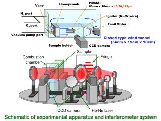
Download
1 / 23
260 likes | 579 Views
LPNHE C. Juramy, D. Martin, H. Lebbolo, P. Antilogus, P. Bailly, R. Sefri, S. Bailey LAL C. de La Taille, F. Wicek, J. Jeglot , M. Moniez, V. Tocut. ASPIC Front-end CCD Readout Circuit For LSST camera. IN2P3 contribution to camera electronics. IN2P3 contribution:

E N D
LPNHE C. Juramy, D. Martin, H. Lebbolo, P. Antilogus, P. Bailly, R. Sefri, S. Bailey LAL C. de La Taille, F. Wicek, J. Jeglot , M. Moniez, V. Tocut ASPICFront-end CCD Readout CircuitFor LSST camera Sefri Rachid @LPNHE La Londe-les-Maures october2009
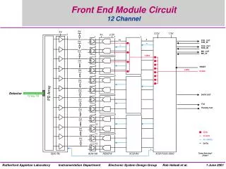
IN2P3 contribution to camera electronics IN2P3 contribution: Video Signal Processing Front End Electronics . .. . CCD Clocks 3 serial 4 parallel 1 reset BackEnd Electronics Back End Module FPGA (1/Raft) Scientific Data 21 Rafts 189 CCD’s 6GB / Frame Clock / DSI Timing / Amplitude SCC CCD 18 bit ADC’s Timing Control Module ASPIC DSI digital 16 outputs 500 X 2K analog -100°C -40°C Warm Electronics Sefri Rachid @LPNHE La Londe-les-Maures october2009
ASPIC: 1rst proto ASPIC: Analog Signal Processing IC • 1rst prototype: mid 2007 to mid 2008 • 2 solutions explored based on ‘Correlated Double Sampling’ • With integrator : Dual Slope Integrator (DSI) • Without integrator : ‘Clamp & Sample’ 4 channels of each on the same silicium substrate to perform crosstalk tests Sefri Rachid @LPNHE La Londe-les-Maures october2009
Vout t reset tfeedthrough Reference level signal level Charge dump ASPIC: 1rst proto Dual Slope Integrator CCD output stage 4 Clocks Clamp & Sample • Requirements: • ~5nV / √Hz • 500KHz Operation freq • .01% Crosstalk • Differential outputs • Output Drive > 50pF • Supply ±2.5V 1 Clock Sefri Rachid @LPNHE La Londe-les-Maures october2009
ASPIC Layout • First proto submited layout • 4 DSI channels • 4 C&S channels • Techno : CMOS 0.35µ 5V • Vendor : AMS • Package : CQFP100 3.8mm 2.7mm Sefri Rachid @LPNHE La Londe-les-Maures october2009
TESTS of ASPIC V1 Sefri Rachid @LPNHE La Londe-les-Maures october2009
COLD TESTS Sefri Rachid @LPNHE La Londe-les-Maures october2009
Power vs Temperature Sefri Rachid @LPNHE La Londe-les-Maures october2009
Offset vs. Temperature Sefri Rachid @LPNHE La Londe-les-Maures october2009
Proto 1 design • The first prototype has demonstrated • Comparison between DSI and C&S in same chip • DSI principle and multi channel IC feasibility at low temperature with low crosstalk • Good fit between simulations and measurements • C&S feasibility Sefri Rachid @LPNHE La Londe-les-Maures october2009
ASPIC: 2nd proto • Technologie : AMS CMOS 0.35µ 5V • 8 Channel full DSI • Package : CQFP100 8 Dual Slope Integrators One ASPIC Channel • 3 input amplifier gains : 2.5 – 5 – 7.5 • to deal with CCD gain spread. • 3 integration time constants : 500ns – 1µs – 1.5µs • to deal with CCD readout frequency. • Idle mode :DC current reduction by a factor of 1.000 baseline : { gain 5 + 500ns integration time} Multi Gain Sefri Rachid @LPNHE La Londe-les-Maures october2009
Warm Test Stand Sefri Rachid @LPNHE La Londe-les-Maures october2009
Linearity Sefri Rachid @LPNHE La Londe-les-Maures october2009
Main Improvement : noise Noise simulations of ASPIC 2 @ -100°C 6µV RMS noise for a Time of Integration of 500ns ASPIC Proto2 Noise simulations and measurements of ASPIC 1 19µV RMS noise for a Time of Integration of 500ns Simulation LPNHE Measurement Sefri Rachid @LPNHE La Londe-les-Maures october2009
Crosstalk measurements @ 300K Reset Signal Signal source -100mV pulse ΔV = Crosstalk Adjacent channel output signal X 10 Sefri Rachid @LPNHE La Londe-les-Maures october2009
LAL/LPNHE Cryostats LAL cryostat dedicated to prototyping tests LPNHE cryostat dedicated to prototyping & pre-prod tests • Already cooled down – used for ASPIC1 Sefri Rachid @LPNHE La Londe-les-Maures october2009
CLASSIC • 8 channels Clamp & Sample chip • Pin to pin compatible with ASPIC 2 • 3 bit programmable gain input amplifier • 4 bit programmable output time constant filter to match the readoutfrequency • Twodifferents C&S topologies • Idle mode Sefri Rachid @LPNHE La Londe-les-Maures october2009
CLASSIC Schematic • New functionalities / ASPIC1: • Switched-capacitor gain • Programmable input gain amplifier • Programmable time constant filter • Two different C&S topologies: • 1st : • One channel noise : 3.9 µV • 18mW/channel and < 1% nonliearity • 2nd • Positive gain channel noise : 2.81 µV • Negative gain channel noise : 2.47µV • 18mW/channel and < 1% nonliearity 18
DSI vs C&S • Signal de sortie d’un CCD = signal de faible niveau: • chaque photo-électron produira quelques µV. • Forme du signal complexe – nécessité d’un timing précis Etage de sortie d’un CCD • Le traitement de l’image doit se faire en lisant le niveau de référence et le signal • La différence de ces signaux donnera le nombre d’électrons du pixel lu • Technique: Correlated DoubleSampling Sefri Rachid @LPNHE La Londe-les-Maures october2009
DSI vs C&S • Dual Slope Integrator • Suppression automatique du bruit de reset des CCD • Utilisé dans SNAP: A low power, wide dynamic range multigain signal processor for the SNAP CCD– JP Walder et Al. – NSS Oct 2004. Sefri Rachid @LPNHE La Londe-les-Maures october2009
DSI vs C&S • Clamp & Sample Switch de clamp • Le bruit CCD en kT/C est « clampé » • Simple – robuste – 1 seule horloge nécessaire – indépendant (jusqu’à une certaine limite!) de la fréquence de lecture du CCD. • - Utilisé pour la lecture des CCD de MegaCam (design du groupe électronique de l’IRFFU) Sefri Rachid @LPNHE La Londe-les-Maures october2009
DSI vs C&S Bruit dominé par le bruit thermique haute fréquencede l’étage d’entrée (pas d’intégration) Bruit • On peut montrer que le bruit: • du DSI est équivalent à • du C&S est équivalent à Bruit dominé par le bruit thermique du CCD (si un étage de gain est placé avant l’intégration) Où en = densité de bruit du CCD, S=gain du CCD, ∆T=temps d’intégration, τ=filtre du C&S Sefri Rachid @LPNHE La Londe-les-Maures october2009
Ampli Bloc Sefri Rachid @LPNHE La Londe-les-Maures october2009