Download

1 / 33
340 likes | 518 Views
Full Adder. Section 4.5 Spring, 2014 J.Ou. Schedule. Outline. Review of a Half Adder Full Adder Explanation Step-By-Step Module Writing Four Bit Adder. Derivation of ∑. Question: What primitive best implements ∑ ? Inputs: A, B Outputs: ∑=. Derivation of Carry Out.

E N D
Full Adder Section 4.5 Spring, 2014 J.Ou
Outline • Review of a Half Adder • Full Adder • Explanation • Step-By-Step Module Writing • Four Bit Adder
Derivation of ∑ • Question: What primitive best implements ∑? • Inputs: A, B • Outputs: ∑=
Derivation of Carry Out • Question: What primitive best implements Co? • Inputs: A, B • Outputs: Co =A∙B
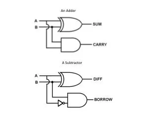
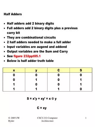
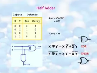
Limitation of a Half Adder A half-adder does not account for carry-in.
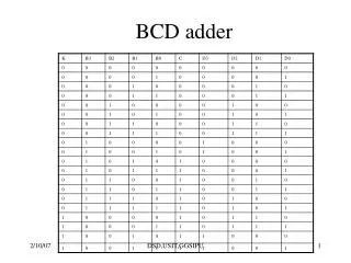
Truth Table for a Full Adder carry-in
Implementation of a Full Adder (carry-in)
Build a Full-Adder Circuit M1 M2 w1 w2 w3
Module Template module module_name ( , , ) endmodule Input, output wires reg Program Body
Module Declaration M1 M2 w1 w2 w3 x,y, and z are the input ports s,c are the output ports wires:x, y,z, s, c wires w1, w2, w3
Module Template module module_name ( , , ) endmodule Input, output wires reg Program Body
Program Body M1 M2 w1 w2 w3 • Use existing half adder cells • Two instances: M1 and M2 • Need an OR gate: • I can use either primitive gates • Use assign statement
Module Test Bench Template //`timescale 1 ms /1 us module module_tb_name ( , , ) endmodule Input, output wires reg Define the test bench Call on the module
Modify half_adder_tb.v Change `include line Change module name
Module Test Bench Template //`timescale 1 ms /1 us module module_tb_name ( , , ) endmodule Input, output wires reg Define the test bench Call on the module
Change input/output, wire/regs • To do list: • Increase X,Y to X,Y,Z • output • t_X,t_Y, t_Z • Question: • Why do we have to use • reg X,Y, but not wire X, Y?
Module Test Bench Template //`timescale 1 ms /1 us module module_tb_name ( , , ) endmodule Input, output wires reg Define the test bench Call on the module
To-Do List Change output file name Add Z to $fmonitor line Read from three bit files Update Z from t_Z Change how the module is invoke.
Program Body M1 M2 w1 w2 w3
Four-Bit Adder G2 G1 G0 G3 C4 is calculated last because it takes C0 8 gates to reach C4. Each FA uses 2 XOR, 2 AND and 1 OR gate. A four-bit adder uses 8 XOR, 8 AND and 4 OR gate.
Output time=230 A0=1 A1=0 A2=0 A3=1 B0=1 B1=0 B2=0 B3=1 C0=0 S0=0 S1=1 S2=0 S3=0 C4=1 time=240 A0=0 A1=1 A2=0 A3=0 B0=0 B1=0 B2=1 B3=0 C0=1 S0=1 S1=1 S2=1 S3=0 C4=0 time=250 A0=0 A1=0 A2=0 A3=1 B0=1 B1=0 B2=0 B3=0 C0=0 S0=1 S1=0 S2=0 S3=1 C4=0 time=260 A0=0 A1=1 A2=1 A3=1 B0=1 B1=1 B2=1 B3=0 C0=0 S0=1 S1=0 S2=1 S3=0 C4=1 time=270 A0=0 A1=0 A2=1 A3=0 B0=0 B1=1 B2=0 B3=0 C0=1 S0=1 S1=1 S2=1 S3=0 C4=0 time=280 A0=1 A1=0 A2=0 A3=0 B0=0 B1=0 B2=0 B3=1 C0=1 S0=0 S1=1 S2=0 S3=1 C4=0 time=290 A0=0 A1=0 A2=0 A3=0 B0=0 B1=0 B2=0 B3=0 C0=1 S0=1 S1=0 S2=0 S3=0 C4=0 time=310 A0=0 A1=0 A2=0 A3=1 B0=1 B1=0 B2=0 B3=0 C0=0 S0=1 S1=0 S2=0 S3=1 C4=0 time=320 A0=1 A1=1 A2=1 A3=0 B0=0 B1=1 B2=1 B3=1 C0=1 S0=0 S1=1 S2=1 S3=0 C4=1 time=330 A0=0 A1=1 A2=0 A3=0 B0=0 B1=0 B2=1 B3=0 C0=1 S0=1 S1=1 S2=1 S3=0 C4=0 time=340 A0=1 A1=1 A2=0 A3=1 B0=1 B1=0 B2=1 B3=1 C0=0 S0=0 S1=0 S2=0 S3=1 C4=1 time=350 A0=0 A1=1 A2=0 A3=1 B0=1 B1=0 B2=1 B3=0 C0=0 S0=1 S1=1 S2=1 S3=1 C4=0 time=360 A0=0 A1=0 A2=0 A3=0 B0=0 B1=0 B2=0 B3=0 C0=1 S0=1 S1=0 S2=0 S3=0 C4=0
Things to Sort Through before writing the module • four_bit_adder.v • What should be declared as inputs? • What should be declared as outputs? • How do I connect the ports of four_bit_add.v module to ports of full_adder.v module? • What should be declared as wires • What verilog modules should I include? • How should the instance be invoked?
Things to Sort Through Before Writing the Module • four_bit_adder_tb.v • What test bench should I use as a template? • What should be the output? • What wires should I have? • What should I replace t_X,t_Y, t_Z with? • How should the four_bit_adder.v be invoked? • How should the output be printed?
What Will Be provided? • Bit files (9 files in all, downloadable from the course website) • half_adder.v • What you need to implement: • full_adder.v • full_adder_tb.v • four_bit_adder.v • four_bit_adder_tb.v • Due date: Next Wed (2/12) in Class.