Download
1 / 1
20 likes | 175 Views
nanoFIP a radiation tolerant FPGA-based WorldFIP agent E.Gousiou , P.Alvarez , E.van der Bij, G.Penacoba , J.Serrano | CERN, Geneva, 2011. User logic. User. User logic. User logic. User logic. User logic. Master. Master. Master. consumption. production. nan FIP. nan FIP.

E N D
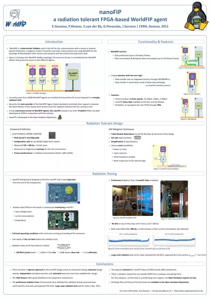
nanoFIP a radiation tolerant FPGA-based WorldFIP agent E.Gousiou, P.Alvarez,E.van der Bij, G.Penacoba, J.Serrano | CERN, Geneva, 2011 User logic User User logic User logic User logic User logic Master Master Master consumption production nan FIP nan FIP nan FIP nan FIP Introduction Functionality & Features • WorldFIP is a deterministic fieldbus used in the LHC for the communication with a variety of systems. Quench Protection, Cryogenics, Power Converters and other critical systems are using WorldFIP for the exchange of data between their sensors and actuators and the control and supervision level. • Figure 1 illustrates the WorldFIP fieldbus topology. The access to the bus is controlled by the WorldFIP Master that grants bus access to the different Agents. • WorldFIP services: • Data production (up to 124 bytes/ frame). • Data consumption & Broadcast data consumption (up to 124 bytes/ frame). Figure 2: Data production & consumption • Simple interface with the User logic: • Data transfer over an integrated memory through WISHBONE or • Data transfer in stand-alone mode (2 bytes data exchange, • no need for memory access). WISHBONE Stand-alone bus Memory Figure 3: User Interface fieldbus TAP sensor actuator sensor JTAG • Features: • Communication at three speeds: 31.25kb/s, 1Mb/s, 2.5Mb/s. • nanoFIP status byte available to the User and the Master. • Possibility to reprogram the User FPGA through JTAG. • Currently, more than 10000 WorldFIP Agents are installed all around the LHC tunnel exposed to a complex radiation field. • Recently, the main provider of the WorldFIP Agent chipset decided to terminate their support; moreover the latest batches of the chipset were proven to be less radiation tolerant than the previous ones. • A new customized version of WorldFIP Agents, the nanoFIP, housed in an Actel ProASIC3 FPGA, has been developed at CERN in cooperation with the industry. • nanoFIP is developed in the Open Hardware Repository. Agent Agent Agent … Figure 4: JTAG feature Figure 1: Fieldbus topology Radiation Tolerant Design • Component Selection • Actel ProASIC3, A3P400, PQFP208 • Flash-based & reconfigurable • Configuration cells do not exhibit Single Event Upsets • Measured TID > 300 Gy > 10 LHC years • Not prone to Single Event Latchups for the LHC environment • Proven performance in radiation environments (ALICE, nQPS, NASA) • SEE Mitigation Techniques • Triple Module Redundancy on all the flip-flops & memories of the design • Fail safe state machines • Simplification of specifications • Various reset possibilities • Power on reset • Input reset pin • Reset broadcast variable • Reset output pin to the external logic User logic Rst Out Rst In PoR Reset Frame Figure 5: nanoFIP reset possibilities Radiation Testing • Preliminary Radiation Tests: 2 nanoFIP chips irradiated • nanoFIP testing board designed so that the nanoFIP chip is well separated • from the rest of the components. • Radiation tests at the Paul ScherrerInstitut: • • 230 MeV proton beam • 1.6e8 cm-2/sec flux• 0.086 Gy/sec dose rate• 5 cm collimator • Another Actel FPGA on the board is continuously monitoring nanoFIP’s • input voltage levels • current consumptions • temperature Figure 6: nanoFIP installed at PSI Figure 7: Closer view of nanoFIP at PSI • No SEU on any of the chips until 7.3e11 p /cm2, 400 Gy • Both chips failed after 400 Gy; a small increase in their current consumption was detected. • Full-load operating conditions with continuous writing and reading of the memories. • Two weeks of dry run tests before the radiation tests. Figure 8: Current consumption (core and IOs) of the 2 nanoFIP chips as a function of TID • Large scale radiation tests of ten chips scheduled for Q4 2011; expected SEU cross section σnanoFIP<~ 1e-13 cm2 Conclusions • There has been a rigorousapproach to the nanoFIP design and to its exhaustive testing; extensive design reviews, independent simulation benches and extended tests over time have validated the design. • The JTAG feature offers great flexibility to the equipment maintenance. • The preliminary radiation tests of two boards have validated the radiation testing setup and have confirmed SEU immunity and expected TID limits. Large scale radiation testswill be made in Dec. 2011. • The expected demand for nanoFIP chips at CERN exceeds 2000 components. • There is already a request for use outside CERN from a company renovating trains. For this company ,as they have to provide long-term support, the Open Hardware aspects are key. • All design files and those of the test board are available in the Open Hardware Repository. • For more information: Eva Gousiou — Eva.Gousiou@cern.ch — http://ohwr.org/projects/cern-fip