Download
1 / 50
500 likes | 594 Views
TWEPP 2011. nan FIP. , a rad-tol FPGA-based WorldFIP agent E. Gousiou, P.Alvarez , E.van der Bij, G.Penacoba , J. Serrano | CERN. Outline. Project Introduction Functionality & Features Design Validation Conclusions. Outline. Project Introduction

E N D
TWEPP 2011 nan FIP , a rad-tol FPGA-based WorldFIP agent E. Gousiou, P.Alvarez, E.van derBij, G.Penacoba, J. Serrano | CERN
Outline Project Introduction Functionality & Features Design Validation Conclusions
Outline Project Introduction Functionality & Features Design Validation Conclusions
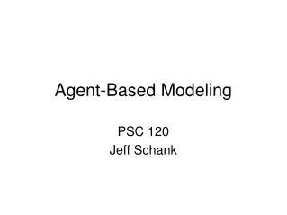
WorldFIP, microFIP & nanoFIP (I) • WorldFIP is a real-time fieldbus used at CERN's LHC for a variety of control systems: Cryogenics, Power Converters, Quench Protection, Beam Instrumentation, Radiation Monitoring, Survey • More than 10000 WorldFIP client nodes (agents) and 200 WorldFIP master nodes installed in the LHC • WorldFIP was selected because of the good performance of its agents under radiation WorldFIP Architecture User logic User logic User logic sensor actuator sensor WorldFIP Master WFIP agent WFIP agent WFIP agent FIELDBUS …
WorldFIP, microFIP & nanoFIP (II) • However, in 2009 Alstom decided to phase out WorldFIP support • Moreover, the latest batches of WorldFIP agents, the microFIP chipsets, were found less radiation tolerant • Finally, it was decided to in-source this technology at CERN • The first phase of in-sourcing concerns the most critical part, the WorldFIP agents is the replacement of microFIP. It implements a subset of microFIP’s functionality. It is a radiation tolerant FPGA-based chip that acts as an agent for the communication over the WorldFIPfieldbus. • The development has been divided to work packages that have been distributed among CERNgroups and industry • Until recently, Alstom was the main provider of WorldFIP technology nan FIP
Open Hardware • nanoFIP is part of the Open Hardware Repository • Public specification, design files and production files • Focus on peer reviews • Better hardware • See also “Open Hardware for CERN’s Accelerator Control Systems”, Erik van der Bij
Outline Project Introduction Functionality & Features Design Validation Conclusions
Functionality & Features User Master consumption n WorldFIPservices: • Data consumption & Broadcast data consumption(up to 124 bytes) • Data production(up to 124 bytes) • Communication in 3 speeds: 2.5 Mbps, 1 Mbps, 31.25 Kbps
Functionality & Features User Master production n WorldFIPservices: • Data consumption & Broadcast data consumption(up to 124 bytes) • Data production(up to 124 bytes) • Communication in 3 speeds: 2.5 Mbps, 1 Mbps, 31.25 Kbps • microFIP: 120 bytes for shared produced and consumed data
Functionality & Features User Master n • Simple interface with the user: • Data transfer over an integrated memory or User WISHBONE MEMORY n WorldFIPservices: • Data consumption & Broadcast data consumption(up to 124 bytes) • Data production(up to 124 bytes) • Communication in 3 speeds: 2.5 Mbps, 1 Mbps, 31.25 Kbps • microFIP: 120 bytes for shared produced and consumed data
Functionality & Features User Master n • Simple interface with the user: • Data transfer over an integrated memory or WISHBONE MEMORY User n 16 bit DATA BUS • Data transfer in 16 in, 16 out lines (no need for memory access) • microFIP: proprietary interface WorldFIPservices: • Data consumption & Broadcast data consumption(up to 124 bytes) • Data production(up to 124 bytes) • Communication in 3 speeds: 2.5 Mbps, 1 Mbps, 31.25 Kbps • microFIP: 120 bytes for shared produced and consumed data
Functionality & Features User Master n • Simple interface with the user: • Data transfer over an integrated memory or User WISHBONE MEMORY n 16 bit DATA BUS • Data transfer in 16 in, 16 out lines (no need for memory access) • microFIP: proprietary interface • JTAG feature • Efficient way to remotely reprogram the user FPGA • 3’ for Actel A3P400; 1.5’ for Xilinx XC5VFX70T User TAP JTAG n • microFIP: no reprogramming feature User TAP WorldFIPservices: • Data consumption & Broadcast data consumption(up to 124 bytes) • Data production(up to 124 bytes) • Communication in 3 speeds: 2.5 Mbps, 1 Mbps, 31.25 Kbps • microFIP: 120 bytes for shared produced and consumed data
Radiation tolerant design • Component Selection • Actel ProASIC3 family • Flash-based & reconfigurable • Configuration cells do not exhibit SEUs • Immune to SELs for the LHC • Measure TID > 300Gy > 10 LHC years • Proven performance in radiation • environments (ALICE, nQPS, NASA). • Mitigation Techniques • Simplification of specifications
Radiation tolerant design • Component Selection • Actel ProASIC3 family • Flash-based & reconfigurable • Configuration cells do not exhibit SEUs • Immune to SELs for the LHC • Measure TID > 300Gy > 10 LHC years • Proven performance in radiation • environments (ALICE, nQPS, NASA). • Mitigation Techniques • Simplification of specifications • TMR of the flip-flops & memories • Fail-safe state machines FPGA area usage
Radiation tolerant design • Component Selection • Actel ProASIC3 family • Flash-based & reconfigurable • Configuration cells do not exhibit SEUs • Immune to SELs for the LHC • Measure TID > 300Gy > 10 LHC years • Proven performance in radiation • environments (ALICE, nQPS, NASA). • Mitigation Techniques • Simplification of specifications • TMR of the flip-flops & memories • Fail-safe state machines FPGA area usage
Radiation tolerant design • Component Selection • Actel ProASIC3 family • Flash-based & reconfigurable • Configuration cells do not exhibit SEUs • Immune to SELs for the LHC • Measure TID > 300Gy > 10 LHC years • Proven performance in radiation • environments (ALICE, nQPS, NASA). • Mitigation Techniques • Simplification of specifications • TMR of the flip-flops & memories • Fail-safe state machines FPGA timing
Radiation tolerant design • Component Selection • Actel ProASIC3 family • Flash-based & reconfigurable • Configuration cells do not exhibit SEUs • Immune to SELs for the LHC • Measure TID > 300Gy > 10 LHC years • Proven performance in radiation • environments (ALICE, nQPS, NASA). • Mitigation Techniques • Simplification of specifications • TMR of the flip-flops & memories • Fail-safe state machines FPGA timing
Radiation tolerant design • Component Selection • Actel ProASIC3 family • Flash-based & reconfigurable • Configuration cells do not exhibit SEUs • Immune to SELs for the LHC • Measure TID > 300Gy > 10 LHC years • Proven performance in radiation • environments (ALICE, nQPS, NASA). • Mitigation Techniques • Simplification of specifications n • TMR of the flip-flops & memories • Fail-safe state machines • Various reset possibilities User Rst Out Rst In PoR Reset Frame
Outline Project Introduction Functionality & Features Design Validation Conclusions
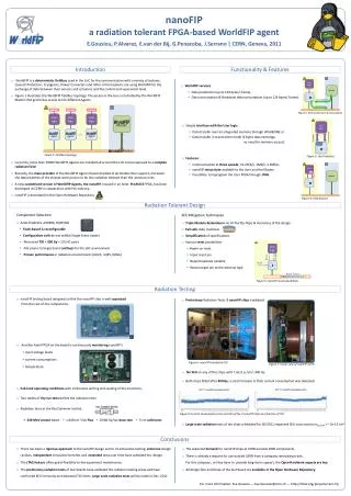
Design Validation Design validation with independent simulation test bench Extensive 5-day VHDL code review by 5 design experts from 2 different CERN groups 19 boards running continuously since May 2011 Test board for functionality & radiation testing developed by external company
Design Validation – Test Board FIELDBUS nan FIP Master User logic Field TR Fiel drive
Design Validation – Test Board Cons FIELDBUS nan FIP Master User logic Field TR Fiel drive
Design Validation – Test Board Prod Cons FIELDBUS nan FIP Master User logic Field TR Fiel drive
Design Validation – Test Board Control Room FIELDBUS nan FIP Master User logic Field TR Fiel drive
Design Validation – Test Board Control Room FIELDBUS nan FIP Master User logic Field TR Fiel drive
Design Validation – Test Board Control Room FIELDBUS nan FIP Master User logic Field TR Fiel drive
Design Validation – Test Board Control Room FIELDBUS nan FIP Master • 9V User logic 50m Field TR Fiel drive
Design Validation – Test Board Control Room FIELDBUS nan FIP Master • 9V • RS 232 User logic 50m 50m Field TR Fiel drive
Radiation Testing Campaigns Large scale tests: Cross section estimation Preliminary tests: qualification of test setup and first understanding of possible failures Extra tests: Irradiation of the nanoFIP, FIELDRIVE & the FIELDTR Study of the effects of high temperature while irradiating
Preliminary Radiation Tests at PSIApril 2011 • 2 nanoFIP chips • Use of the entire Produced and Consumed memory of nanoFIP • 5ms and 500ms macrocycles PSI facility 230 MeV p+ beam p+ beam p+ beam
Preliminary Radiation Tests at PSI – nanoFIPApril 2011 • Correct frames exchange until ~400 Gy; no SEE • At ~400 Gy no frame was being received by the Master; chips not responding • Soft reset/ power cycle not able to recover the functionality • Several hours later without radiation the chips had annealed and were fully functional nanoFIP consumption DUT a [mA] nanoFIP consumption DUT b [mA] “The instabilities were always accompanied by an increase of the current in the FPGA core from 1 to 33 mA.” Radiation-Tolerant ProASIC3 FPGAs Radiation Effects ACTEL report
Preliminary Radiation Tests at PSI – FIELDRIVEApril 2011 • 1 set of FIELDRIVE/ FIELDTR • 5 ms macrocycle • Testing stopped at 400 Gy due to beam time expiration • No error appeared throughout the testing FIELDRIVE consumption DUT a [mA] 10 % current consumption increase
Large Scale Radiation Tests -Target Cross SectionScheduled for Nov 2011 PSI facility, p+ 230MeV Irradiation of 10 devices 400 Gy ProASIC3 lifetime σnanoFIP~ 1e-13 cm2 2e9 p+/cm2/ Gy LHC σnanoFIP~ 1e-13 cm2 < 10 SEE / year 2000 nanoFIPs in the LHC
Outline Project Introduction Functionality & Features Design Validation Conclusions
Conclusions Rigorous design process Exhaustive testing Wide collaboration across the organization and with the industry Expected demand at CERN > 2000 chips The public nature of the design has attracted a European company for train infrastructure
nanoFIP project status Extras
Considerations • During the reprogramming process, the normal gateway tasks will be stopped • Reprogramming will only be used without LHC beam • ProASIC3 devices can be reprogrammed before the accumulation of ~100 Gy
JTAG programmer SW • During the reprogramming process, the normal gateway tasks will be stopped • Reprogramming will only be used without LHC beam • ProASIC3 devices can be reprogrammed before the accumulation of ~100 Gy Master .svf Lib(X)SVF ISC TMS TDI TDO TMS TDI
JTAG programmer SW Master .svf Lib(X)SVF ISC TMS TDI TDO TMS TDI TMS TDI TMS TDI …
JTAG programmer SW Master .svf Lib(X)SVF ISC TMS TDI TDO TMS TDI TDO FSS Ctrl CRC FES TMS TDI TMS TDI TMS TDI …
JTAG programmer SW Master FIELDBUS .svf Lib(X)SVF ISC user TMS TDI TDO FSS Ctrl CRC FES TMS TDI TMS TDI TMS TDI …
JTAG Controller HW FIELDBUS Master user Field TR Fiel drive
JTAG Controller HW Cons FIELDBUS Master user Field TR Fiel drive
JTAG Controller HW Cons Prod FIELDBUS Master user TCK TAP TMS TDI TDO Field TR Fiel drive
JTAG Controller HW Cons Prod FIELDBUS Master user TCK TAP TMS TDI TDO TDO Field TR Fiel drive
nanoFIP vs. microFIP • Tailored to users’ needs • Common use of the chip and centralized support • rad-tol by design • nanoFIPs and microFIPs can co-exist under the same Master • Expected demand >2000 components nan FIP nan FIP Master is not: • Backwards compatible for the user user logic sensor microFIP Signal Conditioner Signal Conditioner Signal Conditioner sensor sensor is:
nanoFIP vs. microFIP • Tailored to users’ needs • Common use of the chip and centralized support • rad-tol by design • nanoFIPs and microFIPs can co-exist under the same Master • Expected demand >2000 components nan FIP nan FIP Master is not: • Backwards compatible for the user nanoFIP user logic sensor Signal Conditioner Signal Conditioner Signal Conditioner sensor sensor is:
Project Organization & Some History ALSTOM-CERN contract with CERN purchasing ALSTOM’s design information. (2008) Concerns for the long-term availability of ALSTOM’s components; WorldFIP Taskforce set up. (2006) Project divided in different Work Packages: (2009) WP1: microFIP code preliminary interpretation (B. Todd, TE/MPE &E. van der Bij) WP2: project management documentation for the in-sourcing (E. van der Bij) WP3: functional specifications for microFIP’s replacement (E. van der Bij) WP4: rewrite & extend microFIP VHDL code WP5: write new code (P. Alvarez & E. Gousiou) WP6: test bench creation (G. Penacoba, TE/CRG) WP7: design of a board for functional and radiation tests (HLP, France) WP8: Radiation tests (CERN RadWGEN/STI & E. Gousiou) Taskforce conclusions: No technological alternative & in-sourcing of WorldFIP technology. (2007)
WorldFIP Frames Communication throughput for 1Mbps: Master -> nanoFIP FSS 2 bytes FSS 2 bytes Ctrl 1 byte Ctrl 1 byte Id 2 bytes Id 2 bytes CRC 2 byte CRC 2 byte FES 1 byte FES 1 byte 8bytes * 8 bits* 1 us 10 us 10 us turnaround time FSS 2 bytes FSS 2 bytes Ctrl 1 byte Ctrl 1 byte Data 2 bytes Data 124 bytes CRC 2 byte FES 1 byte CRC 2 byte FES 1 byte nanoFIP -> Master 130 bytes * 8 bits * 1us 1.1 ms for 124 data-bytes = 0.9 Mb/s Master -> nanoFIP 10 us turnaround time 138 us for 2 data-bytes = 0.1 Mb/s nanoFIP -> Master
Project Status Majority voter circuit: