Download
1 / 34
380 likes | 591 Views
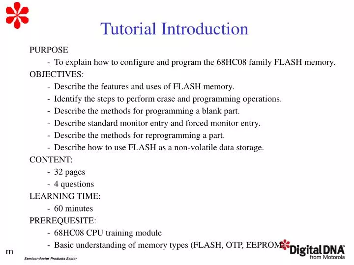
Tutorial Introduction. PURPOSE To explain how to configure and program the 68HC08 family FLASH memory. OBJECTIVES: Describe the features and uses of FLASH memory. Identify the steps to perform erase and programming operations. Describe the methods for programming a blank part.

E N D
Tutorial Introduction • PURPOSE • To explain how to configure and program the 68HC08 family FLASH memory. • OBJECTIVES: • Describe the features and uses of FLASH memory. • Identify the steps to perform erase and programming operations. • Describe the methods for programming a blank part. • Describe standard monitor entry and forced monitor entry. • Describe the methods for reprogramming a part. • Describe how to use FLASH as a non-volatile data storage. • CONTENT: • 32 pages • 4 questions • LEARNING TIME: • 60 minutes • PREREQUESITE: • 68HC08 CPU training module • Basic understanding of memory types (FLASH, OTP, EEPROM)
FLASH Memory Features • In-circuit programming in both user and monitor modes • Small-block programming and erase capability • Internal charge pump sources programming voltage • Built-in FLASH security feature • Block protection against code modification
Split-gate FLASH Advantages • Faster programming time (30-40uS per byte) • Better endurance - 10,000 program/erase cycles • Simpler programming algorithm • More flexible block protection • Efficient single-byte programming
68HC908GP32 FLASH Memory Map User defined Interrupt & Reset Vectors 0xFFF6 - 0xFFFD Monitor Mode entry code addresses 0xFFDC - 0xFFFF Block Protect Register 0xFF7E FLASH Control Register 0xFE08 User FLASH memory 0x8000 - 0xFDFF
FLASH Control Register (FLCR) HVEN — High-Voltage Enable Bit 1 = High voltage enabled to array and charge pump on 0 = High voltage disabled to array and charge pump off
FLASH Page Erase Operation 1. Set ERASE bit and clear the MASS bit in the FLCR 2. Read the FLBPR 3. Write any data to any FLASH address within the page to be erased 4. Delay for tnvs (min 10 uS) 5. Enable the high voltage by setting the HVEN bit in the FLCR 6. Delay for tERASE (min 1 mS) 7. Clear the ERASE bit in the FLCR 8. Delay for tnvh (min 5 uS) 9. Turn off high voltage by clearing the HVEN bit in the FLCR 10. Delay for trcv (min 1 uS) then memory can be accessed again in read mode
FLASH Mass Erase Operation 1. Set ERASE bit and the MASS bit in the FLCR 2. Read the FLBPR 3. Write any data to any FLASH address within the FLASH address range 4. Delay for tnvs (min 10 uS) 5. Enable the high voltage by setting the HVEN bit in the FLCR 6. Delay for tMERASE (min 4 mS) 7. Clear the ERASE bit in the FLCR 8. Delay for tnvhl (min 100 uS) 9. Turn off high voltage by clearing the HVEN bit in the FLCR 10. Delay for trcv (min 1 uS) then memory can be accessed again in read mode
FLASH Program Operation 1. Set PGM bit in the FLCR 2. Read the FLBPR 3. Write any data to any FLASH address within the row to be programmed 4. Delay for tnvs (min 10 uS) 5. Enable the high voltage by setting the HVEN bit in the FLCR 6. Delay for tPGS (min 5 uS) Program Steps
FLASH Program Operation (cont.) Program Steps 7. Write data to the FLASH address to be programmed 8. Delay for tPROG (30-40 uS) 9. All Bytes Programmed? No Yes 10. Clear the PGM bit in the FLCR 11. Delay for tnvh (min 5 uS) 12. Turn off high voltage by clearing the HVEN bit in the FLCR 13. Delay for trcv (min 1 uS) then memory can be accessed again in read mode
FLASH Block Protect Register (FBPR) Address: $FF7E Initial value from factory is $FF.
68HC08 Monitor Features • Single port pin used for serial communications • Normal user-mode pin functionality • Monitor commands • - READ, WRITE, IREAD, IWRITE, READSP, RUN • Execution of code in RAM or FLASH • FLASH memory programming interface • - Programming out-of-circuit • - Programming in-circuit • FLASH memory security
Monitor Mode Commands Command Description Opcode Data returned Operand READ Read byte from memory $4A Returns contents of specified address 2-byte address in high- byte:low-byte order WRITE Write byte to memory $49 None 2-byte address in high-byte:low-byte order; low-byte followed by data byte IREAD Read next 2 bytes in memory from last address accessed $1A Returns next 2 bytes in memory from last address accessed 2-byte address in high- byte:low-byte order IWRITE Write to last address accessed + 1 $19 None Single data byte READSP Reads stack pointer $0C Returns 2-byte address of stack pointer in high-byte:low-byte order None RUN Executes PULH and RTI instructions $28 Executes PULH and RTI instructions None
FLASH Programming • Programming a blank part • - Out-of-circuit monitor mode • - In-circuit monitor mode with standard monitor entry • - In-circuit monitor mode with forced monitor entry • Reprogramming a part • - User mode • - User mode and monitor mode • - Monitor mode with standard monitor entry
Out-of-circuit Programming Tools See: http://www.mcu.motsps.com/documentation/68HC08/devhc08.html
Monitor Mode Entry • Set pins to specific voltages during reset • Standard monitor entry • - Supported in all 68HC08 devices • - Device can be clocked at user mode frequencies • - Select the clock frequency based on desired baud rate • Forced monitor entry • - Includes a simplified interface • - Referred to as “FLASHwire programming” • Security feature • - Valid code entered: memory read, erase, and • programming are available • - Invalid code entered: only mass-erase is available • - Access to other device modules is unaffected
908GP32 Monitor Mode Circuit See figure on page 17
Forced Monitor Entry Overview • Supported in most HC908 devices. • Monitor mode is entered automatically when the reset vector • is blank. • JL3 doesn’t require additional configuration. • GP32 requires these additional configurations: • - Apply voltage to IRQ. • - Set A7 to VSS. • Not supported in 908AZ60 and 908RK2. • Consult the device technical data book for information.
VDD GND IRQ PTA0 PTA7 RESET OSC GP32 ISP Interface VTST or VDD • GP and GR families: • Clock with 9.8304 MHz oscillator • (IRQ = VDD) • Clock with 32.768 kHz crystal • (IRQ = VSS) OSC1
VDD GND IRQ PTA0 PTA7 RESET OSC GP32 ISP Interface (cont.) • GP and GR families: • Clock with 9.8304 MHz oscillator • (IRQ = VDD) • Clock with 32.768 kHz crystal • (IRQ = VSS) OSC1
In-circuit Programming Tools • In most cases, you can use out-of-circuit programming tools. • 68HC08 ICS systems: • - Can be configured to program a device on a target board. • - Supports the mon08 standard mode entry interface. • - Prevents signal contention at the target. • JL3 and JK3 ICS systems (ICS08JLJK): • - Uses a minimum pin interconnection. • - Hardware and user must prevent signal contention. • 908AZ60: • - No ICS system available. • - Can use SPGMR08 to connect the target and a PC • running MCUscribe. • Under special circumstances, write your own host program. • - Host program must adhere to monitor mode requirements. • - See application note AN1770.
Reprogramming with User Mode VDD GND IRQ RXD TXD RESET OSC VDD SCI Clock with any suitable oscillator or crystal Program with 32.768 kHz Crystal Program with 9.8304 MHz Oscillator OSC1
Reprogramming with User and Monitor Modes • 1. In user mode: • - clear the reset vector to make the part appear blank, or • - use a mass erase operation. • 2. Reset the part, then enter monitor mode using forced monitor • entry. • 3. In monitor mode, program the part. • Preferred method under these circumstances: • - Port pin connections are established. • - Device doesn’t include SCI and RAM is small
Reprogramming with Standard Monitor Entry VDD GND IRQ PTA0 PTA7 RESET OSC PTC0 PTC3 PTC1 VTST Clocking with 9.8304 MHz Oscillator OSC1
Reprogramming Methods Summary • Method 1 - User mode • - Preferred method to reprogram a part in-circuit. • - Provides efficient and robust asynchronous communication. • - Can be used with or without an SCI. • Method 2 - User and monitor modes (forced monitor entry) • - Uses forced monitor mode entry. • - Can be used when device doesn’t include SCI and RAM is small. • Method 3 - Monitor mode (standard monitor entry) • - Requires you to satisfy all standard entry requirements. • - If the reset vector is not blank, you must apply VTST to IRQ. • - Doesn’t automatically employ the PLL.
ROM-Based FLASH Programming Routine Function (See AN1831 for Complete Description)
Using FLASH as a Non-Volatile Data Storage • 10,000 program/erase cycles • Short program time • Ability to program one byte at a time • Only page or mass erasing is available • Includes software overhead
Example: Data Storage in FLASH 1st Save 8th Save Indicator Data01 Data02 . . . Data15 Indicator Data01 Data02 . . . Data15 Indicator Data01 Data02 . . . Data15 Indicator Data01 Data02 . . . Data15 Indicator Data01 Data02 . . . Data15 Indicator Data01 Data02 . . . Data15 Indicator Data01 Data02 . . . Data15 Indicator Data01 Data02 . . . Data15 Data Block1 Data Block 2 Data Block 3 Data Block 4 Data Block 5 Data Block 6 Data Block 7 Data Block 8 Data Page -- 128 Bytes
Question Which of the bit strings configures the FLCR for FLASH page erase operations? Click on your choice. a) ‘00001111’ b) ‘00001110’ c) ‘00000110’ d) ‘00001010’
Question In the 908GP32 device, when the FLBPR is set to $02, what range of FLASH addresses is protected? Click on your choice. a) The entire FLASH block is protected. b) $8080 - $FFFF c) $8100 - $FFFF d) $FF00 - $FFFF e) The entire FLASH block is unprotected
Question Which method for reprogramming a part offers the most efficient and robust asynchronous communication? Click on your choice. a) Reprogramming in user mode b) Reprogramming in user and monitor modes c) Reprogramming in monitor mode with standard entry
Question Which of the following features make split-gate FLASH a good choice for non-volatile data storage? Click on your best choice. a) Better endurance (10,000 program/erase cycles) b) Ability to program one byte at a time c) Short programming time d) All of the above
Tutorial Completion • - FLASH Memory Uses and Features • - Erase and Programming Operations • - Programming a Blank Part. • - Monitor Mode Entry • - Reprogramming a Part • - Using FLASH as a Non-Volatile Data Storage