Download
1 / 38
380 likes | 506 Views
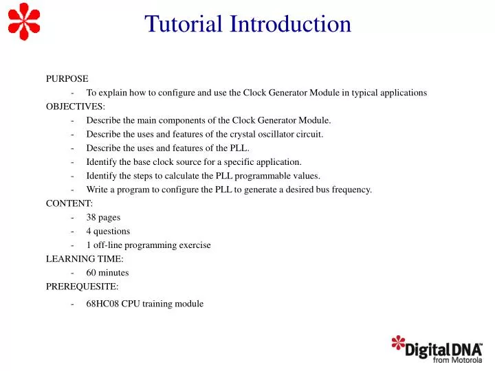
Tutorial Introduction. PURPOSE To explain how to configure and use the Clock Generator Module in typical applications OBJECTIVES: Describe the main components of the Clock Generator Module. Describe the uses and features of the crystal oscillator circuit.

E N D
Tutorial Introduction PURPOSE • To explain how to configure and use the Clock Generator Module in typical applications OBJECTIVES: • Describe the main components of the Clock Generator Module. • Describe the uses and features of the crystal oscillator circuit. • Describe the uses and features of the PLL. • Identify the base clock source for a specific application. • Identify the steps to calculate the PLL programmable values. • Write a program to configure the PLL to generate a desired bus frequency. CONTENT: • 38 pages • 4 questions • 1 off-line programming exercise LEARNING TIME: • 60 minutes PREREQUESITE: • 68HC08 CPU training module
CGMC Features • PLL with programmable output frequency • Low-frequency crystal operation • Programmable prescaler • VCO for low-jitter operation • Automatic bandwidth control mode • Automatic frequency lock detector • CPU interrupt on entry or exit from locked condition • CGMC operation can be enabled during stop mode
CGMC Block Diagram OSC2 OSC1 CGMXCLK CGMRDV Reference Divider VDDA CGMXFC VSSA RDS3-RDS0 CGMOUT VPR1-VPR0 Internal Bus Frequency ¸2 Phase Detector Loop Filter VCO Clock Select ¸2 PLL Analog SIMDIV2 BCS VRS7-VRS0 Lock Detector Automatic Mode Control Interrupt Control CGMVCLK LOCK AUTO ACQ PLLIE PLLF Frequency Divider Frequency Divider CGMVDV MUL11-MUL0 PRE1-PRE0
Crystal Oscillator CircuitFeatures • Used by other MCU modules for precise timing. • Duty cycle is not guaranteed to be 50%. • Can take crystal or external oscillator as source. • Crystal sources must be between 30 kHz to 100 kHz. • External oscillator with PLL enabled must be between 30 kHz • and 1.5 MHz. • External oscillator with PLL disabled must be between DC and • 32.8 MHz.
Crystal Oscillator Circuit OSC2 C2 RS OSC1 X1 CGMXCLK RB C1 CGMXCLK The crystal frequency must be between 30 kHz and 100 kHz to guarantee proper operation PLL PLL (enabled or disabled)
External Oscillator OSC2 OSC1 CGMXCLK Oscillator CGMXCLK PLL The oscillator frequency must be between 30 kHz and 1.5 MHz to guarantee proper operation (enabled)
PLL Features • Generates programmable VCO, CGMVCLK. • Operates in acquisition or tracking mode. • Acquisition mode makes large corrections to VCO. • Tracking mode makes fine adjustments to VCO. • Switches between modes automatically or manually. • Advantages of using a PLL: • Achieve a high bus-frequency using a low-cost crystal • Low-frequency crystals consume less power • Low-frequency crystals provide higher noise immunity
PLL Circuits CGMXCLK CGMRDV Reference Divider Reference Divider VDDA CGMXFC VSSA RDS3-RDS0 VPR1-VPR0 Base Clock Select Circuitry Phase Detector Phase Detector Loop Filter Loop Filter VCO VCO PLL Analog VRS7-VRS0 Lock Detector Lock Detector Automatic Mode Control Interrupt Control LOCK AUTO ACQ PLLIE PLLF Modulo VCO Frequency Divider Frequency Divider Frequency Prescaler Frequency Divider CGMVDV CGMVCLK MUL11-MUL0 PRE1-PRE0
Base Clock Selector CircuitSIM Clock Divider CGMXCLK CGMOUT Internal Bus Frequency 2 Clock Select 2 CGMVCLK SIMDIV2 BCS SIMDIV2
Clock Generator Module R E L N P OSC2 OSC1 CGMXCLK CGMRDV Reference Divider VDDA CGMXFC VSSA RDS3-RDS0 CGMOUT VPR1-VPR0 Internal Bus Frequency ¸2 Phase Detector Loop Filter VCO Clock Select ¸2 PLL Analog SIMDIV2 BCS VRS7-VRS0 Lock Detector Automatic Mode Control Interrupt Control CGMVCLK LOCK AUTO ACQ PLLIE PLLF Frequency Divider Frequency Divider CGMVDV MUL11-MUL0 PRE1-PRE0
Programming the PLL Steps 1-3 of 11 1. Select the bus frequency, fBUSDES. 2. Calculate the VCO frequency, fVCLKDES= 4XfBUSDES. 3.Select a practical PLL (crystal or oscillator) reference frequency, fRCLK, and the reference clock divider, R, where 1 < R < 15. Frequency errors to the PLL are corrected at a rate of . Also, the VCO must be an integer multiple of this rate, where N and P are both integers.
Programming the PLL Current N Value P 0 < NNmax 0 Nmax < N 2Nmax 1 2 2Nmax < N 4Nmax 4Nmax < N 8Nmax 3 Steps 4 and 5 of 11 4. Select a modulo VCO frequency divider, N, where 1 < N < 4095. 5. Select the frequency prescaler, P, where 0 < P < 3. If N Nmax, use P = 0. If N > Nmax, use the table to select P: and then recalculate N:
Programming the PLL Frequency Range E 0 < fVCLK< 9,830,400 0 9,830,400 fVCLK < 19,660,800 1 19,660,800 fVCLK < 39,321,600 2 Steps 6 and 7 of 11 6. Calculate fVCLK and fBUS. 7. Select the VCO power-of-two range multiplier E, where 0 < E < 2: Note: Do not program E to a value of 3
Programming the PLL Steps 8 and 9 of 11 8.Select a VCO linear range multiplier, L, where fNOM= 38.4 kHz and 1 < L < 255. 9. Calculate the VCO programmed center-of-range frequency, fVRS. This is the midpoint between the minimum and maximum PLL frequencies, 38.4 kHz fVRS 40 MHz. For proper operation,
Programming the PLL Steps 10 and 11 of 11 10.Verify the choice of P, R, N, E, and L by comparing f VCLK to f VRS and f VCLKDES . For proper operation, f VCLK must be within the application’s tolerance of f VCLKDES , and f VRS must be as close as possible to f VCLK . 11. Program the PLL registers accordingly: • Select P using PRE bits in the PLL control register (PCTL). • Select E using the VPR bits in the PLL control register (PCTL). • Select N using the PLL multiplier select register low (PMSL) and the PLL multiplier select register high (PMSH). • Select L using the PLL VCO range select register (PMRS). • Select R using the PLL reference divider select register (PMDS).
Example Calculations Steps 1-3 of 11 Step 1: The desired bus frequency is fBUSDES = 8 MHz Step 2: The desired VCO frequency is fVCLKDES = 4 x fBUSDES = 32 MHz Step 3: Let’s choose the reference frequency, fRCLK = 32.768 kHz. Since 30 kHz < fRCLK< 100 kHz, set R = 1.
Example Calculations Current N Value P 0 < NNmax 0 Nmax < N 2Nmax 1 2 2Nmax < N 4Nmax 3 4Nmax < N 8Nmax Steps 4 and 5 of 11 Step 4: Calculate the VCO frequency multiplier, N: rounding up, N = 977. Step 5: Since N < Nmax = 4095, then the frequency prescaler P. P = 0
Example Calculations Frequency Range E 0 £ FVCLK < 9,830,400 0 9,830,400 £ FVCLK < 19,660,800 1 19,660,800 £ FVCLK < 39,321,600 2 Steps 6 and 7 of 11 Step 6: Compare the VCO and bus frequency with the chosen values: Step 7: Select the VCO power-of-two range multiplier E. E = 2
Example Calculations Steps 8 and 9 of 11 Step 8: Calculate the VCO linear range multiplier L, and round to L = 208. Step 9: fVRS, is within the appropriate range, 38.4 kHz fVRS 40 MHz. and the second equation is also satisfied, 65200 76800
Example Calculations Steps 10 and 11 of 11 Step 10: fVRS must be as close as possible to fVCLK, fVRS = 31.9488 MHz fVCLK = 32.014 MHz Step 11: Configure the registers using these values: R = 1PMDS Register N = 0x03D1PMSL & PMSH Registers P = 0PCTL Register E = 2PCTL Register L = 0xD0PMRS Register
Generating Bus Frequency R = 1 R E = 2 E L = 208 L N = 977 N P = 0 P OSC2 fRCLK = 32.768 kHz OSC1 CGMXCLK CGMOUT CGMRDV Reference Divider fNOM = 38.4 kHz fRDV = 32.768 kHz VDDA CGMXFC VSSA RDS3-RDS0 CGMOUT VPR1-VPR0 Internal Bus Frequency ¸2 Phase Detector Loop Filter VCO Clock Select ¸2 PLL Analog 8 MHz SIMDIV2 BCS BCS = 0 VRS7-VRS0 Lock Detector Automatic Mode Control Interrupt Control Power-on Reset CGMVCLK fVCLK = 32.014 MHz LOCK AUTO ACQ PLLIE PLLF fVDV = 32.768 kHz Frequency Divider Frequency Divider CGMVDV 32.014 MHz MUL11-MUL0 PRE1-PRE0
CGMC Registers • PLL control register (PCTL) • PLL bandwidth control register (PBWC) • PLL multiplier select register high (PMSH) • PLL multiplier select register low (PMSL) • PLL VCO range select register (PMRS) • PLL reference divider select register (PMDS)
PLL Control Register(PCTL) PLLIE — PLL Interrupt Enable Bit 1 = PLL interrupts enabled 0 = PLL interrupts disabled
PLL Bandwidth Control Register(PBWC) AUTO — Automatic Bandwidth Control Bit 1 = Automatic bandwidth control 0 = Manual bandwidth control
PLL Multiplier Select Register (PMSH and PMSL) PMSH PMSL MUL11–MUL0 — Multiplier Select Bits These read/write bits control the high and low bytes of the modulo feedback divider that selects the VCO frequency multiplier N. Reset initializes the registers to $0040 for a default multiply value of 64.
PLL VCO Range Select Register (PMRS) VRS7–VRS0 — VCO Range Select Bits These read/write bits control the hardware center-of-range linear multiplier L. A value of $00 disables the PLL and clears the BCS bit in the PCTL. Reset initializes the register to $40 for a default range multiply value of 64.
PLL VCO Range Select Register (PMRS) RDS3–RDS0 — Reference Divider Select Bits Selects the modulo reference divider that programs the reference division factor, R. Reset selects default divide value of 1.
PLL Configuration Flowchart Start PLLON = 0 ; Turn PLL OFF for initialization in PCTL PLLIE = 0 ; Disable PLL interrupts in PCTL P PCTL ; Program P value ; Program E value E PCTL ; Program N value N PMSH:PMSL ; Program L value L PMRS ; Program R value R PMDS AUTO = 1 ; Allow automatic acquisition & tracking PLL Locked? PLLON = 1 ; Turn PLL ON in PCTL No Yes BCS = 1 ; Select PLL as Source of the Base Clock End
Question When using an external oscillator with the PLL enabled, what is the range for the external oscillator frequency? Click on your choice. a) 30 kHz - 100 kHz b) 30 kHz - 1.5 MHz c) 100 kHz - 1.5 MHz d) DC - 32.8 MHz
Question Which of the features represents an advantage of using a PLL in your MCU? Click on the best choice. a) Provides a low-cost method for achieving a high bus-frequency. b) Consumes less power. c) Provides higher noise immunity. d) Generates a programmable output frequency. e) All of the above.
Question To achieve a bus frequency of 4 MHz, what value should you program the VCO power-of-two range multiplier, E, to? Click on your choice. a) 0 b) 1 c) 2
Question What is the bus frequency when the BCS bit set to 1, the PLL is enabled, and the hardware center-of-range linear multiplier, L, set to a non-zero value? Click on your choice. a) CGMXCLK b) CGMVCLK c) CGMXCLK d) CGMVCLK e) none of the above
PLL Programming Exercise • Write a program to configure the 68HC908GP32 PLL • Generate a bus frequency of 8 MHz (32 MHz oscillator • frequency). • Assume XTAL=32.768 kHz. • Write a subroutine to configure the PLL and use polling to • check the lock. • Output a 500 kHz square signal through port C.
Solution: MCU Initialization * ------------------------------------------------------------------- * 68HC908GP32 Initialization * ------------------------------------------------------------------- MOV #%00001011,CONFIG1 ; Configure the CONFIG1 Register ; \\\\\\\\______________ COP Module disabled ; \\\\\\\______________ STOP Instruction Enabled ; \\\\\\______________ Stop mode recovery after 4096 CGMXCLK cycles ; \\\\\______________ LVI operates in 5V mode ; \\\\______________ LVI module enabled ; \\\______________ LVI module Resets enabled ; \\______________ LVI disabled during STOP mode ; \______________ COP time period 262,128 cycles MOV #%00000011,CONFIG2 ; Configure the CONFIG2 Register ; \\\\\\\\______________ Internal Bus Clock used as a source for SCI ; \\\\\\\______________ Oscillator enabled to operate during Stop Mode ; \\\\\\______________ Voltage regulator ON (Vdd > 3.6v) ; \\\\\______________ Unimplemented CLRA ;Initialize the Accumulator LDHX #ENDRAM ;Stack Pointer -> End of RAM TXS ; (H:X -> SP) ; END MCU Initialization
Solution: Main Program * ------------------------------------------------------------------- * Application * ------------------------------------------------------------------- JSR ConfigPLL ; Configure PLL MOV #$FF,DDRC ; Enable Port C as output Toggle: COM PORTC ; 8-cycles loop NOP ; Toggles the PortC every 1µs (1MHz) BRA Toggle ; which generates a 500kHz square signal * END Application
Solution: ConfigPLL Subroutine * ---------------------------------------------------------------------------------- * Subroutine to Configure the PLL via Polling @32Mhz with a 32.768kHz crystal * ---------------------------------------------------------------------------------- ConfigPLL: MOV #%00000010,PCTL ; Configure the PLL Control Register ; \ \ \\\\______________ Program VCO Power-of-two multiplier(E=2) ; \ \ \\_______________ Program Frequency Power-of-two Divider(P=0) ; \ \_________________ Turn PLL off, so it can be initialized ; \__________________ Disable PLL interrupts MOV #$03,PMSH ; Program the Modulo VCO Frequency Divider Value, N MOV #$D1,PMSL ; at the PLL Multiplier Select Registers (N=0x03D1) MOV #$D0,PMRS ; Program the VCO Linear Range Multiplier Value, L ; at the PLL VCO Range Select Register(L=0xD0) MOV #$01,PMDS ; Program the Reference Clock Divider Value, R ; at the PLL Reference Divider Select Register (R=1) BSET AUTO,PBWC ; Allow automatic acquisition & tracking BSET PLLON,PCTL ; Turn PLL ON BRCLR LOCK,PBWC,* ; Wait while PLL locks VCO's desired frequency BSET BCS,PCTL ; When locked, selects PLL as Source of the base clock RTS * END ConfigPLL
Tutorial Completion - CGMC Uses and Features - CGMC components - Base clock selection - PLL Configuration - Programming the PLL