Download
1 / 70
840 likes | 1.17k Views
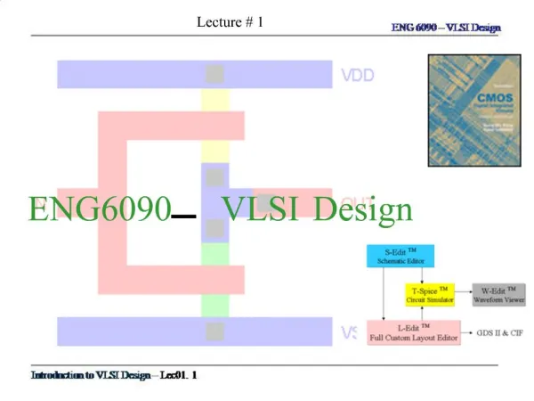
VLSI Design. Presented by P.Sarvani Department of ECE. Dopants. Silicon is a semiconductor Pure silicon has no free carriers and conducts poorly Adding dopants increases the conductivity Group V: extra electron (n-type) Group III: missing electron, called hole (p-type). nMOS Operation.

E N D
VLSI Design Presented by P.Sarvani Department of ECE
Dopants • Silicon is a semiconductor • Pure silicon has no free carriers and conducts poorly • Adding dopants increases the conductivity • Group V: extra electron (n-type) • Group III: missing electron, called hole (p-type) Digital Design
nMOS Operation • Body is commonly tied to ground (0 V) • When the gate is at a low voltage: • P-type body is at low voltage • Source-body and drain-body diodes are OFF • No current flows, transistor is OFF Digital Design
Transistors as Switches • We can view MOS transistors as electrically controlled switches • Voltage at gate controls path from source to drain Digital Design
CMOS Inverter Digital Design
Inverter Cross-section • Typically use p-type substrate for nMOS transistors • Requires n-well for body of pMOS transistors Digital Design
Inverter Mask Set • Transistors and wires are defined by masks • Cross-section taken along dashed line Digital Design
Fabrication Steps • Start with blank wafer • Build inverter from the bottom up • First step will be to form the n-well • Cover wafer with protective layer of SiO2 (oxide) • Remove layer where n-well should be built • Implant or diffuse n dopants into exposed wafer • Strip off SiO2 Digital Design
Oxidation • Grow SiO2 on top of Si wafer • 900 – 1200 C with H2O or O2 in oxidation furnace Digital Design
Photoresist • Spin on photoresist • Photoresist is a light-sensitive organic polymer • Softens where exposed to light Digital Design
Lithography • Expose photoresist through n-well mask • Strip off exposed photoresist Digital Design
Etch • Etch oxide with hydrofluoric acid (HF) • Seeps through skin and eats bone; nasty stuff!!! • Only attacks oxide where resist has been exposed Digital Design
Strip Photoresist • Strip off remaining photoresist • Use mixture of acids called piranah etch • Necessary so resist doesn’t melt in next step Digital Design
n-well • n-well is formed with diffusion or ion implantation • Diffusion • Place wafer in furnace with arsenic gas • Heat until As atoms diffuse into exposed Si • Ion Implanatation • Blast wafer with beam of As ions • Ions blocked by SiO2, only enter exposed Si Digital Design
Simplified Design Rules • Conservative rules to get you started Digital Design
Complementary CMOS • Complementary CMOS logic gates • nMOS pull-down network • pMOS pull-up network • a.k.a. static CMOS Digital Design
Example: NAND3 • Horizontal N-diffusion and p-diffusion strips • Vertical polysilicon gates • Metal1 VDD rail at top • Metal1 GND rail at bottom • 32 l by 40 l Digital Design
I-V Characteristics • In Linear region, Ids depends on • How much charge is in the channel? • How fast is the charge moving? Digital Design
Channel Charge • MOS structure looks like parallel plate capacitor while operating in inversion • Gate – oxide – channel • Qchannel = CV • C = Cg = eoxWL/tox = CoxWL • V = Vgc – Vt = (Vgs – Vds/2) – Vt Cox = eox / tox Digital Design
Carrier velocity • Charge is carried by e- • Carrier velocity v proportional to lateral E-field between source and drain • v = mE m called mobility • E = Vds/L • Time for carrier to cross channel: • t = L / v Digital Design
nMOS Linear I-V • Now we know • How much charge Qchannel is in the channel • How much time t each carrier takes to cross Digital Design
Example • Example: a 0.6 mm process from AMI semiconductor • tox = 100 Å • m = 350 cm2/V*s • Vt = 0.7 V • Plot Ids vs. Vds • Vgs = 0, 1, 2, 3, 4, 5 • Use W/L = 4/2 l Digital Design
Capacitance • Any two conductors separated by an insulator have capacitance • Gate to channel capacitor is very important • Creates channel charge necessary for operation • Source and drain have capacitance to body • Across reverse-biased diodes • Called diffusion capacitance because it is associated with source/drain diffusion Digital Design
Gate Capacitance • Approximate channel as connected to source • Cgs = eoxWL/tox = CoxWL = CpermicronW • Cpermicron is typically about 2 fF/mm Digital Design
Diffusion Capacitance • Csb, Cdb • Undesirable, called parasitic capacitance • Capacitance depends on area and perimeter • Use small diffusion nodes • Comparable to Cg for contacted diff • ½ Cg for uncontacted • Varies with process Digital Design
RC Delay Model • Use equivalent circuits for MOS transistors • Ideal switch + capacitance and ON resistance • Unit nMOS has resistance R, capacitance C • Unit pMOS has resistance 2R, capacitance C • Capacitance proportional to width • Resistance inversely proportional to width Digital Design
Introduction • Chips are mostly made of wires called interconnect • In stick diagram, wires set size • Transistors are little things under the wires • Many layers of wires • Wires are as important as transistors • Speed • Power • Noise • Alternating layers run orthogonally Digital Design
Wire Capacitance • Wire has capacitance per unit length • To neighbors • To layers above and below • Ctotal = Ctop + Cbot + 2Cadj Digital Design
Lumped Element Models • Wires are a distributed system • Approximate with lumped element models • 3-segment p-model is accurate to 3% in simulation • L-model needs 100 segments for same accuracy! • Use single segment p-model for Elmore delay Digital Design
Crosstalk • A capacitor does not like to change its voltage instantaneously. • A wire has high capacitance to its neighbor. • When the neighbor switches from 1-> 0 or 0->1, the wire tends to switch too. • Called capacitive coupling or crosstalk. • Crosstalk effects • Noise on nonswitching wires • Increased delay on switching wires Digital Design
Coupling Waveforms • Simulated coupling for Cadj = Cvictim Digital Design
Introduction • What makes a circuit fast? • I = C dV/dt -> tpd (C/I) DV • low capacitance • high current • small swing • Logical effort is proportional to C/I • pMOS are the enemy! • High capacitance for a given current • Can we take the pMOS capacitance off the input? • Various circuit families try to do this… Digital Design
Pseudo-nMOS • In the old days, nMOS processes had no pMOS • Instead, use pull-up transistor that is always ON • In CMOS, use a pMOS that is always ON • Ratio issue • Make pMOS about ¼ effective strength of pulldown network Digital Design
Dynamic Logic • Dynamic gates uses a clocked pMOS pullup • Two modes: precharge and evaluate Digital Design
Pass Transistor Circuits • Use pass transistors like switches to do logic • Inputs drive diffusion terminals as well as gates • CMOS + Transmission Gates: • 2-input multiplexer • Gates should be restoring Digital Design
Sequencing • Combinational logic • output depends on current inputs • Sequential logic • output depends on current and previous inputs • Requires separating previous, current, future • Called state or tokens • Ex: FSM, pipeline Digital Design
Sequencing Overhead • Use flip-flops to delay fast tokens so they move through exactly one stage each cycle. • Inevitably adds some delay to the slow tokens • Makes circuit slower than just the logic delay • Called sequencing overhead • Some people call this clocking overhead • But it applies to asynchronous circuits too • Inevitable side effect of maintaining sequence Digital Design
Sequencing Elements • Latch: Level sensitive • a.k.a. transparent latch, D latch • Flip-flop: edge triggered • A.k.a. master-slave flip-flop, D flip-flop, D register • Timing Diagrams • Transparent • Opaque • Edge-trigger Digital Design
Latch Design • Buffered output + No backdriving • Widely used in standard cells + Very robust (most important) • Rather large • Rather slow (1.5 – 2 FO4 delays) • High clock loading Digital Design
Sequencing Methods • Flip-flops • 2-Phase Latches • Pulsed Latches Digital Design
Summary • Flip-Flops: • Very easy to use, supported by all tools • 2-Phase Transparent Latches: • Lots of skew tolerance and time borrowing • Pulsed Latches: • Fast, some skew tol & borrow, hold time risk Digital Design
Full Adder Design I • Brute force implementation from eqns Digital Design
Carry-Skip Adder • Carry-ripple is slow through all N stages • Carry-skip allows carry to skip over groups of n bits • Decision based on n-bit propagate signal Digital Design
Tree Adder • If lookahead is good, lookahead across lookahead! • Recursive lookahead gives O(log N) delay • Many variations on tree adders Digital Design
Memory Arrays Digital Design
Array Architecture • 2nwords of 2mbits each • If n >> m, fold by 2k into fewer rows of more columns • Good regularity – easy to design • Very high density if good cells are used Digital Design
6T SRAM Cell • Cell size accounts for most of array size • Reduce cell size at expense of complexity • 6T SRAM Cell • Used in most commercial chips • Data stored in cross-coupled inverters • Read: • Precharge bit, bit_b • Raise wordline • Write: • Drive data onto bit, bit_b • Raise wordline Digital Design
SRAM Sizing • High bitlines must not overpower inverters during reads • But low bitlines must write new value into cell Digital Design
Decoders • n:2n decoder consists of 2n n-input AND gates • One needed for each row of memory • Build AND from NAND or NOR gates Static CMOS Pseudo-nMOS Digital Design
Decoder Layout • Decoders must be pitch-matched to SRAM cell • Requires very skinny gates Digital Design