Download
1 / 1
10 likes | 392 Views
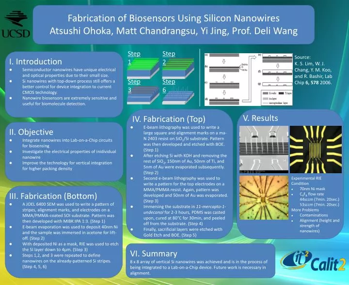
Step 1. Step 2. Source: K. S. Lim, W. J. Chang, Y. M. Koo, and R. Bashir , Lab Chip 6, 578 2006. I. Introduction Semiconductor nanowires have unique electrical and optical properties due to their small size.

E N D
Step 1 Step 2 Source: K. S. Lim, W. J. Chang, Y. M. Koo, and R. Bashir, Lab Chip 6, 578 2006. • I. Introduction • Semiconductor nanowires have unique electrical and optical properties due to their small size. • Si nanowires with top-down process still offers a better control for device integration to current CMOS technology. • Nanowire biosensors are extremely sensitive and useful for biomolecule detection. Step 3 Step 6 Fabrication of Biosensors Using Silicon NanowiresAtsushi Ohoka, Matt Chandrangsu, Yi Jing, Prof. Deli Wang V. Results • IV. Fabrication (Top) • E-beam lithography was used to write a large square and alignment marks on a ma-N 2403 resist on SiO2/Si substrate. Pattern was then developed and etched with BOE. (Step 1) • After etching Si with KOH and removing the rest of SiO2, 150nm of Au, 50nm of Ti, and 5nm of Au were evaporated subsequently. (Step 2) • Second e-beam lithography was used to write a pattern for the top electrodes on a MMA/PMMA resist. Again, pattern was developed and 50nm of Au was evaporated. (Step 3) • Immersing the substrate in 11-mercapto-1-undecanol for 2-3 hours, PDMS was casted upon, cured at 80°C for 30min, and peeled off from the substrate. (Step 4) • Finally, sacrificial layers were etched with Gold Etch and BOE. (Step 5) • II. Objective • Integrate nanowires into Lab-on-a-Chip circuits for biosensing • Investigate the electrical properties of inidividualnanowire • Improve the technology for vertical integration for higher packing density • Experimental RIE Condition • 70nm Ni mask • C4F8 flow rate • 44sccm (7min. 20sec.) • 53sccm (7min. 20sec.) • More Problems • Contaminations • Alignment (height and strength of nanowires) • III. Fabrication (Bottom) • A JOEL 6400 SEM was used to write a pattern of stripes, alignment marks, and electrodes on a MMA/PMMA-coated SOI substrate. Pattern was then developed with MIBK:IPA 1:3. (Step 1) • E-beam evaporation was used to deposit 40nm Ni and the sample was immersed in acetone for lift-off. (Step 2) • With deposited Ni as a mask, RIE was used to etch the SI layer down to 4μm. (Step 3) • Steps 1,2, and 3 were repeated to define nanowires on the already-patterned Si stripes. (Step 4, 5, 6) VI. Summary 8 x 8 array of vertical Si nanowires was achieved and is in the process of being integrated to a Lab-on-a-Chip device. Future work is necessary in alignment.