Download
1 / 42
1.42k likes | 3.32k Views
Lecture 01. VLSI Design Flow. Part 00 of this course. review all what you have learned in digital circuit computer organization/architecture electronics guide you to build your first chip Lab 01: doing Q=|A-B|+|C-D| with one adder build a real chip with UMC 90nm process. ESL design

E N D
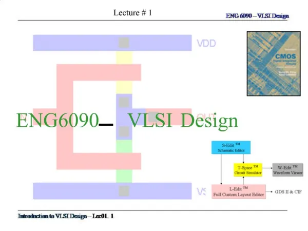
Lecture 01 VLSI Design Flow
Part 00 of this course • review all what you have learned in • digital circuit • computer organization/architecture • electronics • guide you to build your first chip • Lab 01: doing Q=|A-B|+|C-D| with one adder • build a real chip with UMC 90nm process
ESL design (Electronic System Level) RTL design (Register Transfer Level) gate-level design circuit-level design (transistor-level) physical layout Today’s Goal • Review all the hardware courses you have taken in CSIE hardware/software codesign advanced computer architecture computer architecture computer organization digital circuit electronics
ESL design (Electronic System Level) RTL design (Register Transfer Level) gate-level design circuit-level design (transistor-level) physical layout VLSI Design Flow in SoC Era
ESL design (Electronic System Level) RTL design (Register Transfer Level) gate-level design circuit-level design (transistor-level) physical layout Physical Layout
ESL design (Electronic System Level) RTL design (Register Transfer Level) D gate-level design G X X=0 circuit-level design (transistor-level) X=1 physical layout S The basic device to build a chip:MOS transistor
Physical layout of a chip • The image you find in fully-custom design
ESL design (Electronic System Level) RTL design (Register Transfer Level) gate-level design circuit-level design (transistor-level) physical layout Gate-level to Circuit-level Transform
ESL design (Electronic System Level) RTL design (Register Transfer Level) gate-level design circuit-level design (transistor-level) physical layout RTL to Gate-level transform reg A, B, C, D, E; always @(*) E = A&B | C&D;
ESL design (Electronic System Level) RTL design (Register Transfer Level) gate-level design circuit-level design (transistor-level) physical layout More on Behavior/RTL Design the top-level in traditional IC design
B C + Verilog code reg [3:0] A, B, C; always @(posedge clk) begin A <= B+C; end register clk A What is RTL/Behavior design • RTL: Register Transfer Level (Language) • a standard method to design any digital IC • Feature: • designer specify rules to transfer data from one register to another register • EDA (electronic design automation) tool synthesis RTL code to real hardware
What is RTL/Behavior Design • describe the hardware algorithm of the design • looks like something soft, but it’s actually hardware • Example: everything you learned in our “Computer Architecture” course • Booth encoding • Superscalar CPU concept • … • Caution: you should try to transform the behavior to hardware by yourself
ESL design (Electronic System Level) RTL design (Register Transfer Level) gate-level design circuit-level design (transistor-level) physical layout Electronic System Level (ESL) Design
DSP RISC DCT FFT RISC DSP1 DSP2 ESL Design IP Library Design Tools
video frames motion estimation DCT entropy coding Q system-on-chip application algorithm CPU DSP ME memory Transform application algorithm to Silicon SoC (System-on-Chip) • in the SoC era, you have to design both hardware and software! • lots of SW works needs solid HW background • e.g. optimizing compiler design
application algorithm video frames motion estimation DCT entropy coding Q How to make a cell-phone play video? • Step 1: put everything on the CPU as a software program system-on-chip CPU memory
application algorithm video frames system-on-chip motion estimation DCT CPU DSP entropy coding Q ME memory How to make a cell-phone play video? • Step 2: put some specific hardware and move some tasks onto these hardware • do hardware specific program optimization
software application program operating system optimizing compiler architecture design RTL & gate-level design circuit-level design physical level design hardware What a computer architect do • vertical integration of a computer system • from semiconductor to application program
Recall: Ultimate Goal of this course • Let you have the ability to design multi-media SoC chips in the future • featuring complex mathematical computations • Fourier Transform • Discrete Cosine Transform (DCT)
Think of this problem after your finish the course • Consider • fast Fourier transform • discrete cosine transform • …whatever you learned in engineering math… • What’s the most efficient way to realize the transform? • speed, area, power consumption • which part hardware? which part software?
ESL design (Electronic System Level) RTL design (Register Transfer Level) gate-level design circuit-level design (transistor-level) physical layout Cell-Based Design Flow How to realize the flow? the practical aspect
Take a break and read these documents • Document of UMC 90nm cell library • CIC Reference Flow for Cell-Based Design • http://163.25.101.87
Logical synthesis • transform Verilog/VHDL code to gate-level netlist • logic simplification reg D; always @(A or B or C) D = (A&B) | C;
Environment of logical synthesis the Verilog/VHDL you wrote the outcome
Environment of logical synthesis fab dependent (UMC 90nm) well-established gates (AND, OR, etc.)
Environment of logical synthesis set timing and area requirements
Design constraint • you can give such a command to EDA tool: • path delay from A to D < 10ns
Environment of logical synthesis report timing, area, and power consumption
Stage 2: Place & Route direct mapping to the physical view of your chip
Basic scheme of cell-based design • planning on chip area
Basic scheme of cell-based design to place cells area to route wires
Placement • mapping logical gates (cells) onto locations for cells
Routing route wires
Theory about place & route • Optimization issues • timing (path delay) • chip area • power consumption • Theoretical foundation • combinatorial optimization • graph theory • discrete geometry • many many NP-complete problems! • Reference: • S. H. Gerez, Algorithms for VLSI Design Automation, Addison Wesley
Demo: an adder • Let me show you how to build a real chip