Download
1 / 29
300 likes | 430 Views
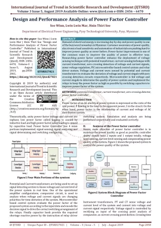
OPERATIONS MANUAL TPF-35 Power Factor Controller For Thyristor Switching Application. TAS Powertek Pvt. Ltd. Corporate Office: W-61, MIDC, Ambad, Nasik - 422010, Maharashtra (India) Tel: +91-(253)-2384038 / 2381090 Email: sales@taspowertek.com. NOTE

E N D
OPERATIONS MANUAL TPF-35 Power Factor Controller For Thyristor Switching Application TAS Powertek Pvt. Ltd.Corporate Office: W-61, MIDC, Ambad, Nasik - 422010, Maharashtra (India)Tel: +91-(253)-2384038 / 2381090Email: sales@taspowertek.com
NOTE These instructions do not purport to cover all details or variations in equipment, nor to provide for every possible contingency to be met in connection with installation, operation or maintenance. Should further information be desired or should particular problems arise which are not covered sufficiently for the purchasers purposes, the matter should be referred to our TAS Powertek Pvt. Ltd. office. The contents of this instruction Manual shall not become part of or modify any prior or existing agreement or relationship. The sales contract contains the entire obligations of TAS Powertek Pvt. Ltd. The warranty contained in the contract between the parties is the sole warranty of TAS Powertek Pvt. Ltd. Any statements contained herein do not create new warranties or modify the existing warranty. The reproduction, transmission or use of this document or its contents is not permitted without express written authority. Offenders will be liable for damages. All rights are reserved.
Index Index Page ---------------------------- 1 Ordering Information ----------------- 2 Features ---------------------------- 3 Specifications ---------------------------- 4 Mechanical Dimensions ------------------ 4 Terminal Arrangement ----------------- 5 Typical wiring diagram ----------------- 6 Front Plate Indications & Keyboard ------- 7 Display screen & default display screen ---- 8 Method for keyboard usage ----------------- 9 Modes of Operation ----------------- 10 Display of various electrical parameters ---- 12 Edit Parameters Mode EDIT: General & IO ----------------- 15 EDIT: System ---------------------------- 16 EDIT: Step ---------------------------- 17 EDIT: Fault ---------------------------- 18 EDIT: Communication ----------------- 20 Annexures Under load kW calculation ----------------- 21 PF correction technique ----------------- 22 Functional block diagram ----------------- 24 APFC panel commissioning instructions Before Power Up ---------------------------- 25 After Power Up ---------------------------- 26 Fault Finding Guidelines ----------------- 27 - 1 -
Ordering Information Product Specific Information Number (PSIN) TPF-35 / nn / Vfb / IL / IC / Aux nnNumber of outputs: 08, 12, 16. VfbFeedback Voltage: 2 – 240Vac 3-phase 4-wire (Line-N) 3 – 415Vac 3-phase 3-wire (Line-Line) Other voltages on request. IL Load current feedback (all 3-phases): 1 – 1Amp.ac CT secondary. 5 – 5Amp.ac CT secondary. IC Capacitor current feedback (all 3-phases): 1 – 1Amp.ac CT secondary. 5 – 5Amp.ac CT secondary. Aux. Auxiliary voltage (single-phase): 2 – 240Vac 1-phase (Line-N) 3 – 415Vac 1-phase (Line-Line) Other voltages on request. - 2 -
Features: • Totally Micro-processor controlled Digital Signal processing • logic for measurements. • All measurements with 1.0 class accuracy. • Automatic Synchronisation capable of giving the correct • results for wrong connections at CT terminals (even wrong • polarity of CTs). • Measurement and kVAr compensation are frequency / THD • compensated. • Load V,I and Cap. current THD measurement with odd • harmonic coeff. upto 15th harmonic. Neutral current analysis • too. • Various modes for switching: • Un-equal(user defined) • C-Series (preset series) • E-Series (user defined) • Output commands: 08, 12 or 16 digital (0V & 12Vdc) outputs. • Fault feedback from individual thyristor switches: Equal • number as per output commands (0V & 12Vdc). • 1 Auxiliary Input with user defined functionality. • Capable of doing the kVAr measurements every cycle of the • mains waveform and provide the kVAr compensation. • Standard 144 X 144 cabinet for panel door flush mounting. • RS232 port with TAS protocol provided on the front fascia. • RS485 port with MODBUS provided on the rear side. • 2MB flash memory built in for data logging. • GSM software built in (can be used by connecting an external • modem to the front RS232 port. • Protections provided (user settable): • Over/under Voltage • Cap. Over/under current / THD. • Over/Under frequency • Over / Under load. • Load unbalance. • Over temperature. • Out of steps (only for indication). • NV-RAM battery down. - 3 -
144 136 150 144 6 Side view Front view • Specifications: • Feed-back Voltage: 240V 3ph 4wire or 415V3ph 3wire with • measurement range of +20% to -40%. • Current input : 1A or 5A for load and capacitor feed-back on • all three phases. • Measurement Accuracy: 1.0% (Dynamic range 10). • Auxiliary Supply: Single phase 240V or 415V with supply • range of +20% to –40%. • Correction time: • Selectable in mains cycles from 1cycle to 250cycles. • RS-232 baud rate selectable upto 57.6kBPS. • Operating temperature: 0 to 70oC. • 1.0 class measurement Operating temperature: 0 to 50oC. • Storage temperature: -10 to +75oC. • Humidity: 0 to 98%. • Supply frequency: 45Hz to 55Hz. • Output commands: 12Vdc solid state 30mA. • Fault feedback: 0 & +12V digital feedback logic. • ‘0’ logic = 0V to +1Vdc. ‘1’ logic = +8Vdc to +14Vdc. • Auxiliary Input: 0 & +12V digital feedback logic. • ‘0’ logic = 0V to +1Vdc. ‘1’ logic = +8Vdc to +14Vdc. Mechanical Dimensions: All dimensions are in mm. Recommended size for cutout on panel door is 138x138-mm. Maximum weight (with clamps and terminals) is 2.5kgs - 4 -
L 1 L 2 CC B+ CC Y+ LC R+ LC Y+ LC B+ CC R+ CC B- CC Y- LC R- LC Y- LC B- CC R- Measurement voltage Auxiliary voltage R Y B Load CT secondary (all three phases) Capacitor CT secondary (all three phases) RS-485 12 VO TOP 8 TFB 4 TOP 13 AI TOP 3 TOP 2 TOP 7 TOP 12 Gnd TFB 5 AI Com TOP 11 TOP 6 TFB 1 TOP 1 TFB 6 TOP 16 TFB 7 TFB 2 TOP 5 12 Vi TOP 15 TOP 10 TOP 4 TFB 8 TOP 9 TFB 3 TOP 14 Gnd Output commands Aux. input TFB 9 TFB 13 TFB 10 TFB 14 TFB 11 TFB 15 TFB 16 TFB 12 Fault feedback input terminals Terminal arrangement: Rear side terminals: The rear side terminals are for measurement voltage input, auxiliary voltage input, load & capacitor CT. Also a second communication port RS-485 is provided on the rear. Bottom side terminals: The bottom side terminals contain the command output terminals and fault feedback input terminals. Auxiliary input terminals are also provided here. - 5 -
Load CT feedback TFB 16 - - - TFB 3 TFB 2 TFB 1 GND 12V o SUPPLY L O A D L 1 L 2 GND 12V i TOP 1 TOP 2 TOP 3 - - - TOP 16 CC B+ CC R+ LC B+ CC Y+ LC Y+ LC R+ LCR- LCY- LCB- CCR- CCY- CCB- Panel incomer R Y B TPF-35 Capacitor current CT feedback Command & feedback TOP 1 TFB 1 GND TOP 2 TFB 2 GND TOP n TFB n GND - - - Step-1 Step-2 Step-n Typical wiring diagram for PF correction: LEGEND: LC Load CT secondary CC Capacitor CT secondary R, Y, B Measurement voltage L1, L2 Auxiliary voltage 12Vi 12V for command TOP 1, 2,…,16 Output commands 12Vo 12V for fault feedback TFB 1, 2,…,16 Fault feedback inputs GND Common ground for command & fault feedback. - 6 -
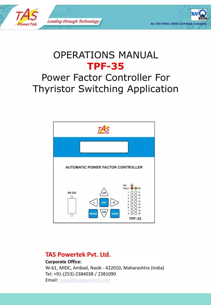
Front plate indications and keyboard: The front fascia contains the keyboard, LCD screen, status indication LEDs & RS232 communication port as shown below. Backlit LCD screen Legends for LED indications: ON, FAULT or DISCHARGING Bank status indication LED Soft touch keypad. RS-232 port Operating keys: The 7 keys are used for following operations: UP To increment numbers; or to go up a menu item; switch ON a bank in manual mode. DN To decrement numbers; or to go down a menu item; to declare a bank fault; switch OFF a bank in manual mode. L To move the cursor to left; or decrease the contrast of LCD screen (possible in default screen). R To move the cursor to right; or increase the contrast of LCD screen (possible in default screen). ENT Enter key. Used to enter a menu or sub-menu; exit the after making data entry to any parameter. MODE To change the mode of operation. SAVE To save the changes made after parameter editing. - 7 -
COSφ=1.000 INDA Symbol LED Description bank is in ON state. bank is in OFF state. bank is declared as FIXED & is in ON state. bank is declared FAULTY & not available for use output stage is not used in the system. bank is in DISCHARGE mode (blinking red LED) COSφ=0.976 INDA Display screen: Symbols on the first line: “COS φ = 1.000” indicates the overall PF of the system. “IND” or “CAP” indicates if this PF is inductive or capacitive respectively. indicates the unit is operating on mains/grid supply. Similarly indicates the unit is operating on generator. “A” or “M” indicates the Auto or Manual mode of operation respectively. Symbols on the second line: The second line indicates the status of each capacitor bank. This status is also provided by LED lamps, as tabulated below: Default Display Screen: Example of a default display screen: Power factor at the load sensing CT is 0.976 inductive (lagging) Unit is operating on mains supply. Unit is operating in Auto mode. Total no. of banks connected are 12. Bank-1 is declared as a fixed bank and is in ON condition. Bank-2, 3, 6 & 7 are variable banks and in ON condition. Bank-4 is declared as faulty. Bank-5 is discharging after switch off. Bank-8, 9, 10, 11 & 12 are in off condition. -8- - 8 -
PRESS If Password Option is Enable / Disable Enter Password: Enable Disable **** PRESS PRESS Default display mode Is PASSWORD correct? Enter the 4 digit Password by using & keys. NO YES * Continued on next page Method of keyboard usage: Flowchart for entering into different modes of operation. At the default display any one of the following three actions can be preformed: Password will be asked if it is enabled. 1) use UP / DN keys to view various electrical parameters. 2) use R / L keys to increase or decrease LCD contrast. 3) press ENT to change the modes of operation (Auto / Manual) OR to enter into the Edit Parameters menu to set the values of various parameters. - 9 -
* Select Select Select 1. Edit Parameter 2. Auto Operation 3. Manual Operation Continued from previous page 1 2 3 4 5 6 7 8 9 10 11 12 13 14 15 16 Default display mode Continued on next page. Modes of operation – Auto / Manual: After entering the Select Parameters mode, use the UP / DN keys to view the following three menu screens. At the required screen & press ENT key to get into that menu. Auto mode: Unit will start operating in Auto mode instantly. Manual mode: After the ENT key is pressed all banks will be switched off. Press ENT key once again. Now the cursor starts blinking at the first bank position. Here use R / L keys to select any particular bank. Use UP key to switch it ON and use DN key to declare it as faulty. To switch off a bank, select it and press DN key. If a bank is already declared faulty, then press DN again to declare it healthy. After setting faulty/healthy status it can be made permanent by saving the setting. To do this press SAVE key. # - 10 -
Select Select 2. Auto Operation 3. Manual Operation # Continued from previous page. Select 1. Edit Parameter Edit Parameters Edit Parameters Edit Parameters Edit Parameters Edit Parameters Fault Step General & IO Communication System Operation in Auto mode Operation in Manual mode General parameters. Supply system & APFC related parameters. COSφ=0.976 INDA COSφ=0.976 INDM Communications related settings. Capacitor bank step settings. Fault trip settings. Back to the modes of operation. The Edit Parameter mode: This mode is used to edit (set) the values of system related various parameters. Details are given from page 14 onwards. - 11 -
Display TAS Powertek Display Display Display Display Power Per-Phase RMS Overall Values TPF-35 1.6.0 Harmonics Energy Overall values gives the average values of system parameters – V, I, kW, kVAr, kVA, Ic, C-kVAr. Load side PF, kVAr, kVA & frequency. Per Phase RMS values of voltage, current, neutral current & capacitor current. Displays per phase values of PF, KW, KVA, KVAR and Capacitive KVAR. Displays overall energy parameters like KWH, Inductive & Capacitive KVARH, KVAH and C-KVARH. Displays per phase THD for V, I, Neutral current & Capacitor as well as odd harmonics up-to 15th. Displays the measured kVAr value of each connected output step. Displays the internal temperature of the unit. Displays current time & date that is set on internal Real Time Clock. Displays the version of software. Display Display Aux Function Step KVAr Time: 12:45:45 Date: 23/06/08 Display of various electrical parameters: Values of various electrical parameters – measured values, PF values, power & energy values and voltage/current harmonic values can be viewed. At the default display screen, use the UP / DN keys to view the following 8-menus. In any of the following menu, press ENT to go into further sub-menu. The list of sub-menus is given in the next page. - 12 -
R-Phase Voltage 00415.0V (L-L) R-Phase PF 1.000 IND Y-Phase Voltage 00415.0V (L-L) Y-Phase PF 1.000 IND B-Phase Voltage 00415.0V (L-L) B-Phase PF 1.000 IND R-Phase Current 1000.0 A R-Phase kW 000250.0 Y-Phase Current 1000.0 A Y-Phase kW 000254.0 B-Phase Current 1000.0 A B-Phase kW 000256.0 Neutral Current 0001.0 A R-Phase kVAr 000005.7 Average Voltage 00415.1V (L-L) R-Phase Cap Cur 0009.5 A Y-Phase kVAr 000006.7 Average Current 1000.5 A Y-Phase Cap Cur 0009.5 A B-Phase kVAr 000005.2 Active Power 000440.0kW B-Phase Cap Cur 0009.0 A R-Phase kVA 000254.0 Reactive Power 000010.0kVAr Y-Phase kVA 000256.0 Apparent Power 000442.0kVA B-Phase kVA 000258.0 Capacitor Current 0009.5 A R-Phase CkVAR 000002.3 C-kVAr 000006.1 Y-Phase CkVAR 000003.1 Load side PF 0.998 IND B-Phase CkVAR 000002.4 Load side kVAr 000016.1 Load side kVA 000438.1 Frequency 50.0 Hz Sub-menus: Per Phase RMS Overall Values Power - 13 -
KWH 000000000.0 Vr-THD-R 000.0% Step[1] kVAr 0010.0 IND KVARH 000000000.0 Vy-THD-R 000.0% Step [2] kVAr 0010.0 CAP KVARH 000000000.0 Vb-THD-R 000.0% Step [3] kVAr 0010.0 KVAH 000000000.0 Ir-THD-R 000.0% Step [4] kVAr 0010.0 C-KVARH 000000000.0 Iy-THD-R 000.0% Step [5] kVAr 0010.0 Ib-THD-R 000.0% Step [6] kVAr 0010.0 Step [7] kVAr 0010.0 In-THD-R 000.0% CCr-THD-R 000.0% Step [8] kVAr 0010.0 CCy-THD-R 000.0% - - CCb-THD-R 000.0% Step [16] kVAr 0010.0 Energy Harmonics Step kVAr Aux Function INT Temperature 00 Deg C Note on Harmonics menu: (1) The “R” in the above parameters refer to the method of THD calculation. R is for RMS. Other option is F, for fundamental. (2) Under each THD menu, further sub-menu is available which gives the individual odd harmonics values from 3rd up to 15th for voltage & currents (load, neutral & capacitor currents) To view these values, press the ENT key at any of the above of the parameters & use UP / DN keys to view from 3rd to 15th harmonic levels. - 14 -
Password Enable : 1 Change password : 0000 Load default No : 0 THD to display R : 0 Reset energy cntr No : 0 Aux I/P function None : 0 Edit Parameters Mode: In this mode, the various system settings can be carried out. To get into this mode from default screen (see page-8), press DN key, select Edit Parameters & press ENT. The following sub-menus can be accessed for editing data: General & IO : for general settings System : for system related setting Communication : for communication setting Step : for capacitor step settings Fault : for setting fault limits To exit any of these sub-menu, press MODE key once. To exit the Edit Parameters menu, press MODE key again. Note: In Edit Parameters menu or sub-menu if no key is pressed for more than a minute, the default display screen comes on & all changes done till then are discarded. Following are the parameters in each of the above menus. General & IO Password: Enable or disable the password. Enable=1, Disable=0. Change password: Set a a new password (4-digit). Load default: Loads factory set default values. Yes=1, No=0. THD to display: Select the type of THD calculation to RMS or Fundamental. RMS-THS=0, Fundamental-THD=1. Reset energy counter: Reset the energy counters. Yes=1, No=0. Aux I/P function: Any one of the three functions can be assigned to aux. input: 0=None. Means input is not used. 1=Enable/Disable the outputs to all the capacitor banks when 12Vdc auxiliary input is given at Aux. Input terminals. - 15 -
Meas. Voltage : 415 Ext PT ratio 0001.0 : 1 Cur CT Primary Mains : 1000 Cur CT Primary Genr : 0500 Cap Cur CT Pri : 1000 PF upper limit Mains [CAP:0] 0.998 PF lower limit Mains [IND:1] 0.998 PF upper limit Genr [CAP:0] 0.998 PF lower limit Genr [IND:1] 0.998 Mains / Generator Mains : 0 Phase Auto Sync. Yes : 1 Auto Sync Flt. Tol (%) : 020 Rst Ph Auto Sync No : 0 2=Mains/Gen. This is used if RTPFC system is used with duel supply system. Unit works with two sets for PF correction. One is mains and another is Generator. ‘1’ at this input will use the Generator Set Points and ‘0’ at this input will use the Mains Set points for PF correction. (Note: with this method, usage of 3Ph summation CTs is mandatory for Source current feed-back). 3=Reset Banks fault. ‘1’ at this input would reset the status of all the faulty banks declared to a normal healthy status. System Meas. Voltage: This is a factory set parameter & is only for viewing. Ext PT ratio: This is by default set to 0001:1. But if external PR is used this ration can be set. Limits 000.1(lower) to 500.0(upper). Cur CT Primary (Mains / Generator): The feedback source (Mains / Genr.) current. Lower 0001, Upper 5000. Cap Cur CT Pri: The feedback source current. Lower 0001, Upper 5000. Power factor limits: Two PF limits can be set for PF correction (lower limit & upper limit). Each of these can be set either inductive or capacitive. Mains / Generator: This parameter is effective only if the aux. Input is not defined in mains/gen. Mode. This parameter defines whether the unit should consider the set points of mains or gen. 0=Mains, 1=Generator. Phase Auto Sync.: Auto synchronisation feature is enabled (1) or disabled (0). Auto Sync. fault: If put in auto-sync, unit carries out some Power parameter checks. In this process, the tolerance of these parameters is defined here. If this tolerance is exceeded then unit declares failure of Auto-Sync. In this condition, unit stops compensating PF correction. Reset Ph Auto Sync.: If auto-sync fault is detected the unit can start normal PF correction if this parameter is set to 1 (yes). Else set to 0(no). - 16 -
Steps connected : 16 Default mode Auto : 0 Compensation kVAr Mean : 1 Cap Bank voltage (L-L) : 00415V Correction time Cycles: 00010 Step response time Cycles: 00045 Fix-bank setting _ _ _ _ _ _ Correction type C-series : 2 C-series : 00 111111 E-series 1 4 8 8 8 8 BIN / C / E series Bank kVAr: 20 Unequal bank [1] kVAr = 001 Unequal bank [2] kVAr = 002 . . . Unequal bank [6] kVAr = 006 Step Steps connected: Defines the number of steps operation. Default mode: This parameter defines the mode of operation during power-up. Default is Auto. Set 0=Auto, 1=Manual. Compensation kVAr: Defines the method for kVAr compensation. Set 0=Instantaneous or 1=Mean. Cap bank voltage: The line-line voltage at which the kVAr is defined. Correction time: Tine between two consecutive kVAr compensations. Step response time: The time after which the kVAr of any step should be measured when the step turns ON. Fix-bank setting: Defines the banks that are to be declared as fixed. Correction type: The unit can have banks of various configuration that are defined by four methods: 0=Binary, 1=Unequal, 2=C series, 3=E series. Binary is in ration of 1:2:4:8:16:32. Unequal is used when there is no definite ratio among the banks. C Series is predefined control series. The standard ratios are preloaded & can be selected here. E Series is user defined control series. Here the user can define their own ratio which are not available in C Series. Here digits 1,2,..9 and A,B,..F (A=10, B=11, C=12, D=13, E=14, F=16) can be used. Bin / C / E bank kVAr: Defines the kVAr of smallest bank (for the value at position 1) of the selected series. Unequal bank kVAr [ ]: If unequal bank correction type is selected, define the kVAr of each step here from 1 up to 16. - 17 -
Over Vol. Fault Disable : 0 Over Vol. limit % : 115 Over Vol. Resume % : 110 Under Vol. fault Disable : 0 Under Vol. limit % : 085 Under Vol. Resume % : 090 Over load fault Disable : 0 Over load limit % : 130 Over load resume % : 125 Under load fault Disable : 0 Under load limit % : 020 Under load resume % : 025 Load unbalance Flt Disable : 0 Load unbalance limit % : 020 Over Cap-I Fault Disable : 0 Fault For most of the faults defined here the options available are as follows: 0=Disable. 1=Indicative. Flash a fault message. 2=Off Step. Switch off non-fixed steps one by one. 3=Fixed Off. Switch off all fixed step. 3=Fast Off Step. Switch off all steps in one shot. For all the faults, normally two limits are defined. One is Detection Limit and other is Resume Limit. If detection limit is exceeded any one of the above action is performed as set by the user. Similarly if the fault limit drops below the resume limit, then the action is deactivated. Over voltage fault: As the name suggests it is for over voltage condition. Under voltage fault: For under voltage. Over load fault: In the event of over load it is some times recommended to remove capacitors from the circuit to reduce the fault current levels. The limits can be set here. Under load fault: The value here is set as the %age of Maximum rated kW. This is useful in case of banks are put in circuit to take care of no-load compensation. Value for this under load kW can be calculated as shown in annexure in annexure on page-19. Load unbalance fault: The limits defined here are in %age of max. of individual phase currents. Capacitor current fault tolerance: This is defined in kVAr which can be deviated. - 18 -
Over Cap-I limit % : 130 Over Cap-I Resume % : 125 Over CC Auto restart Disable : 0 Auto restart time Seconds : 0060 Under Cap-I fault Disable : 0 Under Cap-I limit % : 095 Under Cap-I resume % : 097 Temperature Flt Disable : 0 INT Temperature L. Limit : 50 INT Temperature U. Limit : 60 Cap Cur THD Flt Disable : 0 Cap Cur THD limit % : 010 Cap Cur THD resume % : 008 Step health check Disable : 0 Cap Cur fault Tolerance: 10 Over capacitor current fault: If put in indicative mode it works as normal limit & resume operation. If put is any of the tripping modes, the capacitors are out of circuit. Under this case for restart, Auto-Restart is to be enabled along with the Auto-Restart Time. Note that with Auto-Restart feature enabled & capacitor taking over-current even after restart may put the system in hunting mode. Under capacitor current fault: This fault can be only in two options. 0=Disable, 1=Indicative. This fault is not for tripping the capacitor banks. Thus, here there is no need for Auto-Restart and the unit works with normal limit & resume settings. Internal Temperature Fault: The unit monitors temperature inside it housing. This temperature can go up either due to ambient within the APFC panel or due to component failure within TPF-35. Set upper limit to trip and lower limit to resume. Capacitor current THD: Capacitors are vulnerable to harmonics. The unit can sense the THD value of capacitor current and in case of THD exceeding can give this fault. Step health check: The unit carries out on line monitoring of the kVAr values of every step. This is when the step is put in the circuit. In case the tolerance limit defined here is exceeded, that specific bank is declared faulty. - 19 -
Unit ID : 0000 Baud rate 9600 : 1 Time 01:58:40 Date 01:01:08 Initialize RTC No : 0 Clear NVRAM No : 0 GSM or RS232 RS232 : 0 Service provided 0000000000 SMS receiver no. 0000000000 Out of banks fault Disable : 0 NV RAM batt. Fault Disable : 0 Out of banks fault: This is only with 0=Disable, 1=Indicative options. If set to indicative, the unit will indicate the fault, provided “if in two consecutive correction cycles, the PF is more inductive than lower PF set point and all the healthy capacitor banks are in ON state.” That is if the unit needs more capacitors than available to reach the desired upper PF set point. NV RAM battery fault: Internal battery failure. Communication Unit ID: Value can be 0000 to 9999. Default value 0001. This ID is used for serial communication on RS232 TAS protocol. Baud rate: Selectable: 0=4800bps; 1=9600bps; 2=19200bps; 3=38400bps; 4=57600bps; 5=115200bps. Time: Defines the time setting. Date: Defines the date setting. Initialize RTC: 0=No; 1=Yes. If ‘yes’ it initializes the real time clock. Clear NVRAM: 0=No; 1=Yes. Defining Yes clears the NVRAM (real time clock). This will also clear the energy counters. This is generally used to clear the NVRAM Check sum fault. Press Save after setting this parameter. GSM or RS232: The rear side port can be configured for either GSM by connecting an external GSM modem or as an RS232 port for data downloading. Service provider: Set the GSM service provider number here. Normally 10digit. SMS receiver no.: This defines the number to which the SMS communication is to be sent. Normally it is a master control receiving number. - 20 -
KVAR (Ind) PF LOWER Under Load settings: PF UPPER 1.25 X smallest capacitor bank KW KW Under- Load. No change band. Capacitor Addition band. Capacitor Removal band. KVAR (Cap) For PFUPPER Inductive and PFLOWER Inductive : For PFUPPER Capacitive and PFLOWER Inductive : 1.25 X Smallest bank KVAR. [tan{cos -1(PFUPPER)} + tan{cos-1(PFLOWER)}] 1.25 X Smallest bank KVAR. [tan{cos -1(PFLOWER)} – tan{cos-1(PFUPPER)}] 1.25 X Smallest bank KVAR. [tan{cos -1(PFUPPER)} – tan{cos-1(PFLOWER)}] Under-Load KW value setting = Under-Load KW value setting = Under-Load KW value setting = For PFUPPER Capacitive and PFLOWER Capacitive: Annexure – Under load kW calculation: Following figure depicts the method of under load calculation. - 21 -
PFUPPER & PFLOWER both set as inductive: PFLOWER. PFLOWER. KVAR (Ind) smallest Capacitor bank KVAR X 2 width. PFUPPER. PFUPPER. - KW. KW. KVAR (Cap) No change band. Capacitor Addition band. Capacitor Removal band. PFUPPER as Capacitive & PFLOWER as inductive: KVAR (Ind) smallest Capacitor bank KVAR X 2 width. PFLOWER. PFLOWER. - KW. KW. PFUPPER. PFUPPER. KVAR (Cap) Annexure – PF correction technique: Following figures show the technique of PF correction for various combinations of Inductive & Capacitive settings. Continued… - 22 -
PFUPPER & PFLOWER as Capacitive: KVAR (Ind) smallest Capacitor bank KVAR X 2 width. - KW. KW. PFLOWER. PFLOWER. PFUPPER. PFUPPER. KVAR (Cap) No change band. Capacitor Addition band. Capacitor Removal band. Continued… All the three conditions specified in the diagram, the four quadrant operation is achieved if “Auto-Synchronisation” is not activated. If this feature is activated, the unit works with only kW +ve two quadrants. Thus, for 4 quadrant operations requirements, Auto-Synchronisation should be kept off. Typical example of 4 quadrant operation is with “Co-Generation Plants” and “Wind-Power Generation”. But with most conventional consumer applications, only +ve KW is seen, where the Auto Synchronisation feature can be kept ON. It can be seen that there are two PF set points to be set in the unit - Upper and Lower. The unit ensures that PFUPPER is never exceeded. Additionally, “No change band” to minimum KVAR band size equal to smallest bank KVAR X 2 ensures no hunting during the low KW loading. TPF-35 is normally set for PF settings as per first two diagrams shown where PFLOWER is inductive. This philosophy helps to optimise the system maximum KVAR to be used as well as reduces the number of switching operations during higher loading conditions. This ensures better life expectancies to the switched capacitors as well as to the switching devices. This methodology of KVAR compensation reduces the complex settings that are used by conventional PF relays. The settings like C/K ratio and KVAR offsets/ shifts are eliminated makes the TPF-35 user friendly and thus easy to commission. - 23 -
3 channel load current f.b. 3 channel Voltage f.b. RS-485 port on the rear side. GSM modem drivers. 3 channel capacitor current f.b. V, I, PF and Power Measurement Block For every AC mains Cycle. RS-232 port on front fascia. Keyboard, Display & other support function block. • Calculation • Block for • Energy Parameters • Harmonic analysis Temp. sensor Power Factor Correction Block + event monitoring. Outputs Commands For Capacitor Switching. TPF-35 Power Supply Digital fault feedback input from thyristor switches Onboard relays Capacitor switching commands Thyristor switches fault feedback inputs. Annexure – Functional block diagram: The functional diagram of the TPF-35 power factor controller for thyristor switching application. - 24 -
APFC panel commissioning instructions Before panel is powered up for the first time: 1. Panel Wiring Check Ensure that all connections in the panel is tightened properly and there are no loose connections. Also ensure that the wiring is done as per the wiring diagram. 2. Power Wiring Check Ensure that the power cables are connected properly from the Panel I/C to the feeder I/C or the transformer bushings. The connection has to be after the Load Feed back CT looking from the Transformer side. Ensure that the Bus Bars and/or Lugs are clean and free of Dust, Corrosion or Oxidation on the contact sides so that good electrical connection is maintained. The surface area should be flat so as to get maximum contact area. If required Clean the Bus Bars and/ or Lugs by rubbing it with Polish Paper to remove the oxidation layer. Provide contact paste in between the contacts surfaces. Not performing this, can result in to a weaker source point for Capacitor charging during Step on and this can generate undesirable Noise which can hamper the performance of equipments installed in the capacitor panel. 3. Load Feed Back CT connection Ensure that the load feed back CT connections are done properly. Confirm that correct phase CT is connected with the correct phase input terminals. (Even though auto sync is capable of taking care of wrong CT polarities or CT position interchanging, but then on display, the Phase readings may be seen to be interchanged. (May be R-phase reading would be seen in B-phase and vice-versa. CT connections to be done carefully so as to ensure that the wire does not get open and there is no loose connection. Loose connection or open CT secondary can result in very high voltages getting developed in the circuit which can damage the CT and also produce high levels of noise in the system. - 25 -
After the panel is powered up: • Remove the fuses/switch-off MCBs/MCCBs which are in series with every capacitor bank. Connect supply to the TPF-35. Keep the load feedback and capacitor current feedback in shorted condition. • Turn ON the supply to the panel and set date/time & various other parameters as per the panel configuration. It is important to understand the meaning of every parameter from the instructions given before and then put the appropriate values in them. Wrong values entered can give the wrong performance of the panel. Keep Auto-Synchronisation in Disabled state. • Once the parameterization is complete, put the TPF-35 in Manual mode to check if every bank command is being transmitted to the thyristor switch. This can be observed by the LEDs on the thyristor switches. The corresponding output should be checked for physical turn ON / OFF of the thyristor. • Once all the thyristors are seen to be getting the correct commands, switch off the supply to the panel and replace all the fuses (or turn on MCBs/MCCBs if they are provided instead of fuses). Turn on the panel. • 5. Put TPF-35 back in Manual mode and turn ON/OFF the individual steps. Use Tong tester (ac current measurement) to check that current in all three phase of the corresponding bank are OK. In case any bank is not giving the desired current, check for capacitor bank healthiness or power circuits. • 6. Keep all the banks in off mode. Remove the short of Load feedback CT. In case KW value is seen as –ve for any phase, CT is with wrong polarity. Either select “Auto-synchronisation” in Enable mode or change CT polarity. • 7. Remove the capacitor feedback CT short. Now turn ON the capacitor banks one by one and observe that capacitor current increases as per the rating of the steps on capacitor Current display. Turn ON all the banks to see that almost full rated current flows through the capacitors. • 8. Switch OFF all the banks manually and put the TPF-35 in Automatic mode. Switch Off the supply to panel and put it ON. • If auto-synchronisation is enabled, TPF-35 will first turn ON all the capacitor banks and turn them off. This is one of the routine steps for auto-synchronisation during power up. • In case of message of “Auto-Synchronisation Failure”, TPF-35 will go in “No compensation”. In case of such failures (normally seen with very high fluctuating loads only), manual synchronisation is mandatory by physically checking the CT connections and polarity. • Observe panel performance for about 2hrs after commissioning. - 26 -
Corporate Office/Works/Design Centre: W-61, MIDC, Ambad, Nasik - 422010, Maharashtra (India)Tel: +91-(253)-2384038 / 2381090Email: tas@taspowertek.com Marketing and After-Sales Service:A/58, Kamal Pushpa, K.C. Road, Bandra, Mumbai-400050.Tel: +91-9930513923Email: sales@taspowertek.com Regional Office: Delhi191-B, Ground Floor, Padam Nagar (Filter Market),New Delhi - 110007 (India).Tel: +91-9911615701Email: delhi@taspowertek.com