Download
1 / 23
460 likes | 1.43k Views
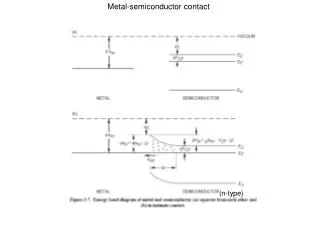
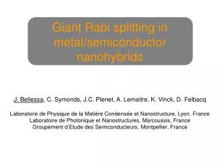
Metal-Semiconductor Interfaces. Metal-Semiconductor contact Schottky Barrier/Diode Ohmic Contacts MESFET. Device Building Blocks. Schottky (MS). p-n junction. HBT. MOS. Energy band diagram of an isolated metal adjacent to an isolated n-type semiconductor.

E N D
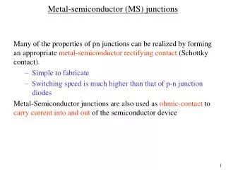
Metal-Semiconductor Interfaces • Metal-Semiconductor contact • Schottky Barrier/Diode • Ohmic Contacts • MESFET ECE 663
Device Building Blocks Schottky (MS) p-n junction ECE 663 HBT MOS
Energy band diagram of an isolated metal adjacent to an isolated n-type semiconductor q(fs-c) = EC – EF = kTln(NC/ND) for n-type = EG – kTln(Nv/NA) for p-type ECE 663
Energy band diagram of a metal-n semiconductor contact in thermal equilibrium. qfBn = qfms + kTln(NC/ND) ECE 663
Measured barrier height fms for metal-Si and metal-GaAs contacts ECE 663 Theory still evolving (see review article by Tung)
Energy band diagrams of metal n-type and p-type semiconductors under thermal equilibrium ECE 663
Energy band diagrams of metal n-type and p-type semiconductors under forward bias ECE 663
Energy band diagrams of metal n-type and p-type semiconductors under reverse bias ECE 663
Charge distribution Vbi = fms (Doping does not matter!) fBn = fms + kTln(NC/ND) electric-field distribution E(x) = qND(x-W)/Kse0 W Em = qNDW/Kse0 (Vbi-V) = - ∫E(x)dx = qNDW2/Kse0 0 ECE 663
Depletion Depletion width q Charge per unit area ECE 663
Capacitance Per unit area: Rearranging: Or: ECE 663
1/C2 versus applied voltage for W-Si and W-GaAs diodes ECE 663
1/C2 vs V • If straight line – constant doping profile – • slope = doping concentration • If not straight line, can be used to find profile • Intercept = Vbi can be used to find Bn ECE 663
Current transport by the thermionic emission process Thermal equilibrium forward bias reverse bias J = Jsm(V) – Jms(V) Jms(V) = Jms(0) = Jsm(0) ECE 663
Note the difference with p-n junctions!! In both cases, we’re modulating the population of backflowing electrons, hence the Shockley form, but… V > 0 V > 0 V < 0 V < 0 • Barrier from metal side is pinned • Els from metal must jump over barrier • Current is limited by speed of jumping • electrons (that the ones jumping from • the right cancel at equilibrium) • Unipolar majority carrier device, since • valence band is entirely inside metal band • Barrier is not pinned • Els with zero kinetic energy can slide • down negative barrier to initiate current • Current is limited by how fast minority • carriers can be removed (diffusion rate) • Both el and hole currents important • (charges X-over and become min. carriers)
Let’s roll up our sleeves and do the algebra !! Jsm= 2qf(Ek-EF)vx = 2q vx > vmin,vy,vz dkxdkydkzvxe-(Ek-EF)/kT (2p)3/W Vbi - V V > 0 Ek-EF = (Ek-EC) + (EC -EF) EC - EF = q(fBn-Vbi) Ek - EC = m(vx2 + vy2 + vz2 )/2 m*vmin2/2 = q(Vbi – V) kx,y,z = m*vx,y,z/ħ ECE 663
This means… ∞ ∞ ∞ Jsm= q(m*)3W/4p3ħ3 dvze-m*vz2/2kT dvxvxe-m*vx2/2kT dvye-m*vy2/2kT -∞ -∞ vmin x e-q(fBn-Vbi)/kT (2pkT/m*) (2pkT/m*) (kT/m*)e-m*vmin2/2kT = (kT/m*)e-q(Vbi-V)kT ∞ ∞ dxe-x2/2s2= s2p dx xe-x2/2s2= s2e-A2/2s2 = qm*k2T2/2p2ħ3e-q(fBn-V)kT -∞ A = A*T2e-q(fBn-V)kT A* = 4pm*qk2/h3 = 120 A/cm2/K2 ECE 663
In regular pn junctions, charge needs to move through drift-diffusion, and get whisked away by RG processes MS junctions are majority carrier devices, and RG is not as critical. Charges that go over a barrier already have high velocity, and these continue with those velocities to give the current
Forward current density vs applied voltage of W-Si and W-GaAs diodes ECE 663
Tunneling through the barrier – high doping Schottky barrier becomes Ohmic !! ECE 663