Download
1 / 13
140 likes | 725 Views
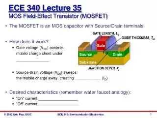
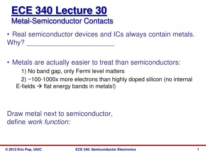
ECE 340 Lecture 30 Metal-Semiconductor Contacts. Real semiconductor devices and ICs always contain metals. Why? _______________________ Metals are actually easier to treat than semiconductors: 1) No band gap, only Fermi level matters

E N D
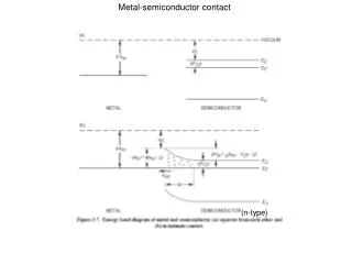
ECE 340 Lecture 30Metal-Semiconductor Contacts • Real semiconductor devices and ICs always contain metals. Why? _______________________ • Metals are actually easier to treat than semiconductors: 1) No band gap, only Fermi level matters 2) ~100-1000x more electrons than highly doped silicon (no internal E-fields flat energy bands in metals!) Draw metal next to semiconductor, define work function:
Another scenario, if Φm < Φs • Contact potential V0 • Use analogy to p+n junction to evaluate depletion width W: • Ex: calculate semiconductor work function qΦs if it is silicon doped p-type with NA=1017 cm-3
Two types of metal-silicon contacts become apparent: 1) Schottky (rectifying, like a diode) 2) Ohmic • How do you get one vs. the other? • When would you want one vs. the other? • Silicon work function: • Some typical metal work functions:
Schottky (rectifying) contact on n-type Si: • Apply V>0 on metal, reduce built-in energy barrier. • What happens? • Can electrons flow from metal to Si? • Apply V<0 on metal, enhance built-in energy barrier. qΦB =
Ohmic contacts on silicon, two ways to achieve them: 1) Choose metal with appropriate work function to “match” the Fermi level of p- or n-type Si 2) Dope silicon highly, to thin out Schottky barrier, so electrons can tunnel through (almost) regardless of Φm
ECE 340 Lecture 31-32Metal-Oxide-Semiconductor (MOS) Capacitor • MOS capacitor, needed for MOSFETs and DRAM (and Flash): • In nMOS device: n+ gate (or low Φm), p-substrate • In pMOS device: p+ gate (or high Φm), n-substrate Note gate = metal by Intel at 45nm tech node, since ~2008. Why? • SiO2 most common gate insulator (EG = 9 eV, εr = 3.9) Intel switched to bilayer HfO2 (EG ≈ 5 eV, εr ≈ 20) with SiO2. Why? d
Metal/high-K MOSFET (we’ll come back to it later): • Draw band diagram of MOS capacitor with n+ gate and p-substrate. source: intel.com
We drew this as n+ gate MOS, but remember that gate can also be metal! Then metal gate work function Φm matters: • Define the bulk (body) potential: • Define the surface potential:
What happens if we apply a gate voltage? • There are two important reference voltages here: 1) Flat-band voltage, VFB = voltage needed on gate to get E-field = 0 everywhere (flat bands). Note, this can be zero (“ideal” MOS), but generally depends on gate Φm or doping, qVFB = 2) Threshold voltage, VT = voltage needed on gate to get electron concentration at Si/SiO2 surface same as that of (majority) holes in the bulk. I.e. Φs(inv) = 2ΦF andSi surface is “inverted”.
In general, voltage applied on the gate will be: • Where Vi = Eid = voltage dropped across SiO2 insulator • And Φs = voltage dropped in the Si (surface potential) • Q: what is Vi when V = VFB? • Three interesting regions of MOS operation: • Accumulation (V < VFB for pMOS) • Depletion (VFB < V < VT) • Inversion (VT < V) • Let’s take them one by one:
Accumulation: V < VFB, holes accumulate at the surface |qVi| Vi
Depletion: VFB < V < VT, holes pushed back in substrate • Surface is depleted of mobile carriers • All surface charge is due to fixed dopant atoms • Again, we apply depletion approximation we used for p-n diode: assume abrupt displaced charge (rectangular). Draw: qVi
Charge density in depleted region: • Poisson’s equation in depleted region: • Integrate twice (from bulk x = W to surface x = 0 to obtain surface Φs or depletion depth W: • To find Φs as a function of gate V we need all voltage drops. • Across insulator: Vi = Eid = Qd/Ci where • Qd is depletion charge in silicon substrate, Qd = -qNAW = • Finally, VG = VFB + Φs + Vi = • We can now solve from the surface potential vs. gate V: