Download
1 / 10
100 likes | 202 Views
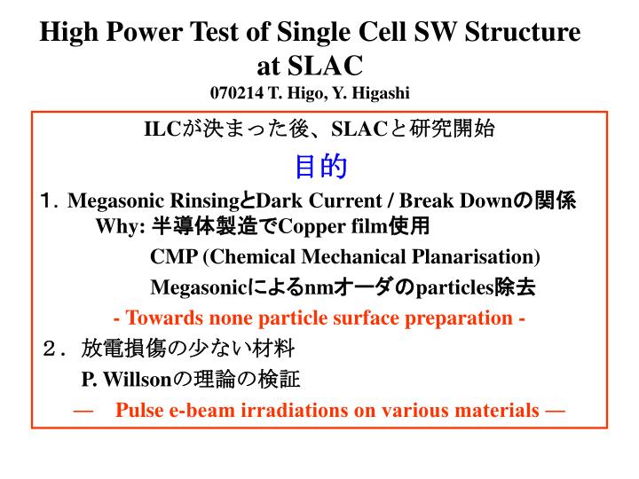
High Power Test of Single Cell SW Structure at SLAC 070214 T. Higo, Y. Higashi. ILC が決まった後、 SLAC と研究開始 目的 1. Megasonic Rinsing と Dark Current / Break Down の関係 Why: 半導体製造で Copper film 使用 CMP (Chemical Mechanical Planarisation) Megasonic による nm オーダの particles 除去

E N D
High Power Test of Single Cell SW Structure at SLAC070214 T. Higo, Y. Higashi ILCが決まった後、SLACと研究開始 目的 1.Megasonic RinsingとDark Current / Break Downの関係 Why: 半導体製造でCopper film使用 CMP (Chemical Mechanical Planarisation) Megasonicによるnmオーダのparticles除去 - Towards none particle surface preparation - 2.放電損傷の少ない材料 P. Willsonの理論の検証 ―Pulse e-beam irradiations on various materials ―
報告の内容 • KEK/SLAC 仕事分担(Budget含む) • Megasonic Technologies • Pulse e-beam irradiation • Tentative High power Test Results at SLAC(DolgachevのSlide紹介) (Testした空洞はKEKから送った後、SLACで真空リーク発生ー>C. Peasonが補修ロー付けー>表面洗浄なし、Bakingのみ) ・ CLIC情報(SLACでもらったSlide) ・ 今後の見通し
研究の進め方 KEK Structure Fabrication, Assembly and Surface Treatment SLAC Design and Experiments (Exp. Scheduleは特に決めていない)
Cu - EEM (CMP(ChemicalMechanicalPlanarization/Polishing)) Done by Koike, Takatomi, Higashi at Toshiba Machine CO on 1995 EEM P-v = 0.1 nm Diamond turning P – v= 20 nm
CMP Mechanism CMP技術大系 (発行:グローバルネット(株))より Cu表面のCMP/洗浄方法が半導体R&Dによりかなり明らかに!!!!
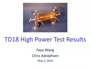
2nd Single Cell SW structure preparation Megasonic rinsing 960kHz, 600 W, 5 minutes operation Ultra Pure Water 18.2 M W, 2 TOC All parts were applied megasonic rinsing Assemble envelopment: Class 10 No vacuum leak 400 degC baking, period : 5days
関連する実験結果との比較 • HPWRによるS-Band空洞の性能(五十嵐、山口氏ら) @ Processing Timeが減少した(~30%) @ Max. 加速勾配の変化ほとんどなし • 埼玉大 DC 放電試験結果 @ 250 MV/m前後で放電 • 今回SLACでの結果(Very Tentative) Dark Current (Field Emissionが多いが. . . . ) @ Acc Gradient was 240MV/m? @ Surface Field seems to be 300MV/m?
今後の見通し • SLACでHigh Power Test中(補修ロー付け品)とMegasonic RinsingしたCellのDark Currentの比較を1ヶ月以内にSLACでおこなう。(結果をみて決めることになる) • New Design of SW structure ( geometries change -> Shintake Cavity?)