Download
1 / 36
360 likes | 528 Views
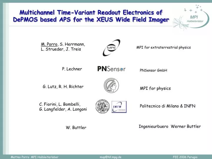
Multichannel Time-Variant Readout Electronics of DePMOS based APS for the XEUS Wide Field Imager. M. Porro , S. Herrmann, L. Strueder, J. Treis. MPI for extraterrestrial physics. P. Lechner. PNSensor GmbH. G. Lutz, R. H. Richter. MPI for physics. C. Fiorini, L. Bombelli,

E N D
Multichannel Time-Variant Readout Electronics of DePMOS based APS for the XEUS Wide Field Imager M. Porro, S. Herrmann, L. Strueder, J. Treis MPI for extraterrestrial physics P. Lechner PNSensor GmbH G. Lutz, R. H. Richter MPI for physics C. Fiorini, L. Bombelli, G. Langfelder, A. Longoni Politecnico di Milano & INFN Ingenieurbuero Werner Buttler W. Buttler Matteo Porro MPI Halbleiterlabor map@hll.mpg.de FEE 2006 Perugia
XEUS project(X-rayEvolvingUniverseSpectroscopy) Exploring the early universe by imaging spectroscopy in the X-ray band (100 eV – 30 keV) Observation of the hot Universe at high redshifts Device active area 7.68 x 7.68 cm2 Device thickness 450 mm Pixel size: 75 x 75 mm2 Position resolution ca. 30 mm Total 1024 x 1024 pixel cells Energy resolution @ Mn-Ka 125 eV Energy resolution @ C-Ka 50 eV System noise 3-5 e- ENC Matteo Porro MPI Halbleiterlabor map@hll.mpg.de FEE 2006 Perugia
XMM EPIC XEUS WFI energy range 0.1 ... 15 keV 0.1 ... 20 keV focal length 7.5 m 50 m angular resolution 15 arcsec 2 arcsec focal plane res. 36 µm / arcsec 250 µm / arcsec field of view 30 arcmin 5 arcmin collection area 1 keV 0.5 m² 6 m² (30 m²) time resolution 70 msec 1 ... 5 msec operating temp. 130 K > 180 K Active Pixel Sensor » 1 preamp / pixel » random accessible pixels » no charge transfer XEUS WFI specifications • Specifications thickness 300 µm ➞500 µm pixel size 150 µm ➞ 75 µm detector area 6 x 6 cm² ➞ 7.68 x 7.68cm² format400 x 400 ➞ 1024 x 1024 readout speed readout speed leakage current Matteo Porro MPI Halbleiterlabor map@hll.mpg.de FEE 2006 Perugia
The DePMOS Concept • p-channel MOSFET integrated on high-ohmic, sideward depleted n-substrate • a potential minimum is formed by S/D potentials aided by a • deep n implantation • electrons are collected in an internal gate close to the surface • the transistor current is modulated by charge collected in the • internal gate • the transistor can be switched on/off by an external (top) gate • An n+ clear contact surrounded by a clear gate is used to remove the charge from the internal gate Matteo Porro MPI Halbleiterlabor map@hll.mpg.de FEE 2006 Perugia
DePMOS Properties • DePMOS provides detection and amplification jointly • DePMOS is free of interconnection capacitances • The internal gate exists regardless of a current flowing in the DePMOS channel or not. Power consuption is minimized • Multiple non-desctructive readout is possible • matrix pixel 75 x 75 µm² • DEPFET • geometry W = 47 µm • L = 5 µm • dedicated technology • 2 polysilicon layers • 2 metal layers • leakage current level • 100 pA/cm² • 16 fA/pixel Matteo Porro MPI Halbleiterlabor map@hll.mpg.de FEE 2006 Perugia
APS – matrix organisation • global contacts for drain (source) , back contact, substrate, … • gate, clear & cleargate connected row-wise • sources connected column-wise • 1 active row • DEPFETs ON » readout & reset • all other pixels • DEPFETs OFF » integration • random accessible pixels • » window mode, mixed mode Matteo Porro MPI Halbleiterlabor map@hll.mpg.de FEE 2006 Perugia
APS for the WFI • APS readout modes 1024 x 1024 pixel 7.68 x 7.68 cm² 5 arcmin FOV • full frame mode • readout time: ~ µsec / row • ~ msec / frame • window mode • mixed mode • fast timing mode • e.g. 16 x 16 pixel • ~ 100.000 cps • »fast transients of • bright point sources Matteo Porro MPI Halbleiterlabor map@hll.mpg.de FEE 2006 Perugia
DEPFET APS – prototypes for the XEUS WFI • Switcher II • 64 channel control chip • 2 ports / channel • integrated sequencer • high voltage CMOS process (> 20 V p-p) • 50 MHz clock • CAMEX 64 G / K • 64 channel low noise voltage amplifier • 64 channel 8-fold CDS filter • 64/1 analog multiplexer • source follower gain 3.7 µV/el. Matteo Porro MPI Halbleiterlabor map@hll.mpg.de FEE 2006 Perugia
incomplete clear! DEPFET – signal measurement(time variant readout) measure signal levels 1. before clear -» signal 2. after clear -» baseline 3. calculate difference Matteo Porro MPI Halbleiterlabor map@hll.mpg.de FEE 2006 Perugia
clear pulses laser pulses drain current output measurements time DePMOS Linearity The drain current is measured Laser intensity is calibrated with an X-ray source Variation of the total charge by increasing number of the laser pulses per cycle • Integral non-linearity <0.4% • input range of 200 keV Matteo Porro MPI Halbleiterlabor map@hll.mpg.de FEE 2006 Perugia
QIN DID DVEG DVEG DVS CEQ=QIN/DEG CEQ=QIN/DEG QIN Front end Configurations and Equivalent Input Capacitance source follower readout drain current readout gm=50mS ID=60mA Charge/current gain (gQ) 200-350pA/el. Charge/Voltage Gain 4-6 mV/el. • The signal and the noise sources are referred to the external gate • Definition of Equivalent Input Capacitance CEQ • QIN in the internal gate -> DVS or DID • DVEG external gain signal that produces the same DVS or DID • CEQ=QIN/DEG Measured CEQ=35-40fF Matteo Porro MPI Halbleiterlabor map@hll.mpg.de FEE 2006 Perugia
Noise Spectral Density • ID 60mA • gm 50mS • √af=3mV • √a=18nV/ √Hz • √(8/3)kT/gm= • =14nV/ √Hz • noise corner 30kHz Matteo Porro MPI Halbleiterlabor map@hll.mpg.de FEE 2006 Perugia
Readout Requirements • DePMOS parameters • CEQ=40fF • gm=50mS • gQ=200pA/el. • V/c=4mV/el. • √a=14nV/ √Hz • √af=3mV • electronics requirements: • multichannel ASIC • time-variant readout • variable readout speed • maximum readout speed 4mS • total ENC <4 el. r.m.s. • dynamic input range: 40keV • Linearity <1% Matteo Porro MPI Halbleiterlabor map@hll.mpg.de FEE 2006 Perugia
ASIC Development • VELA Chip • In collaboration with Politecnico di Milano and INFN (Vlsi ELecrtonics for Astronomy) • AMS 0.35mm CMOS 3.3V • Trapezoidal Weighting Function with • Switched Current Technique • Source Follower readout • Drain Current readout • First submission June 2006 • First prototypes in September 2006 • CAMEX Chip • In collaboration with Mr. W. Buttler • IMS 0.8mm CMOS 5V • 8-fold Multi-correlated Double Sampling • Source Follower readout • First Prototypes already tested • -64 channels • -no adjustable bandwidth • 128 channel version with adjustable bandwidth under design Matteo Porro MPI Halbleiterlabor map@hll.mpg.de FEE 2006 Perugia
MCDS-CAMEX CAMEX 64 G / K • ac-coupled, low noise voltage amplifier • 64 channel parallel 8-fold CDS • internal PMOS current load • integrated CDS sequencer • 64/1 analog output serializer • power consumption ≤ 0.6 W • row processing time ≥ 4 µsec • 128 channel version in design Matteo Porro MPI Halbleiterlabor map@hll.mpg.de FEE 2006 Perugia
Measured ENC on noise peak: 3.6 el. r.m.s. with single pixel hits spectrum 133 eV @ 5.9 keV, T = -40 °C Energy resolution of the matrix Ceq=40fF shaper parameters: A1/t=1.26x106 A2=1.27 cycle time: 16ms Predicted ENC: 3.4 el. r.m.s. Matteo Porro MPI Halbleiterlabor map@hll.mpg.de FEE 2006 Perugia
MCDS Filtering optimization • The used WF has quite high slope • The bandwidth is not optimized for the used speed • Optimizing the bandwidth an ENC of 2.1 el. is predicted • With the used bandwidth it should be possible to read-out the pixel in 4ms • The bandwidth must be adjusted for every speed setting • A scalable trapezoidal WF would provide the near optimum filter for Series noise at every speed setting Matteo Porro MPI Halbleiterlabor map@hll.mpg.de FEE 2006 Perugia
Vout Vout subtraction time time time Trapezoidal WF with SCT 1° integration 2° integration out subtraction Current proportional to the input charge deposited into the DePMOS Double integration of this current Subtraction of the output of the two integrating stages after the first integration The output is maximized when the input signal arrives between the two integration phases (Flat-top region) Vout current proportional to the charge stored into the pixel Matteo Porro MPI Halbleiterlabor map@hll.mpg.de FEE 2006 Perugia
2 3 1 2 1 3 Practical Implementation out integrator stage subtraction stage • the charge integrated in the first integration is transferred to a second stage (subtraction stage) • the first stage is resetted before the second integration • at the end of the second integration the output of the second stage gives the difference between the two integrated values Matteo Porro MPI Halbleiterlabor map@hll.mpg.de FEE 2006 Perugia
MCDS vs SCT • SCT • Benefits: • The equivalent bandwidth is independent from timing • A finite width filter function is feasible • Lower switching noise • Drawbacks: • An offset of the input signal is critical and can heavily deteriorate the dynamic range • The gain depends on the timing (an adjustable gain is needed) • MCDS • Benefits: • The gain is almost independent on the timing • An offset of the input signal is not critical • Drawbacks: • The equivalent bandwidth depends on the timing (An adjustable low-pass filter is needed) • A real finite width WF is not feasible • Higher switching noise Matteo Porro MPI Halbleiterlabor map@hll.mpg.de FEE 2006 Perugia
Bias current source drain source V2I gate drain Bias current subtraction gate Source Follower vs. Current readout • Benefits: • The input signal is AC coupled. It is relatively easy to cope with: • - non homogeneity of the DePMOS matrix • - eventual Vth shifts • Drawbacks: • The speed of the system is limited by the gm of the DePMOS and by the Capacitance of a matrix Source Line (30-40pF) • The voltage step at the source must be converted into a current (more suitable for MCDS) • Only a small signal amplification is possible because of the limited dynamic range Source Follower • Benefits: • The DePMOS drain current is directly used as the input signal of the integrator (pixel gain 200-300 pA/el) • all DePMOS terminals are at a fixed potential • The speed is no more limited by the Source line capacitance • Drawbacks: • It is more complex to cope with the non homogeneity of the Matrix. • A current cancellation circuit is needed for each individual pixel Current Readout Matteo Porro MPI Halbleiterlabor map@hll.mpg.de FEE 2006 Perugia
Vin IOUT Source Follower: V2I M 1 • The output current is not set by a feedback: mismatch can be important • Output current must be in the range of few mA to limit the size of the capacitances of the integration stage • Converted current in injected into the output mirror by a drain (MB drain) • The second pole of the loop gain is given by CF and 1/gmMB. The stability is independent from RV2I that can be high (tens of kW). dominant pole CC CIN 0V 0V MB second pole 0V CF RV2I Matteo Porro MPI Halbleiterlabor map@hll.mpg.de FEE 2006 Perugia
V2I Noise analysis 1 M 4kT/RS in,MIR en,AMP CIN 4kT/RV2I CF RV2I (8/3)kTgm • RS>1/gmDePMOS=20K ->RS>100K • en,AMP at the input. gmAMP 10mS W/L 800/.5 • RV2I attenuated by (CF/CIN)2=100 RV2I=16K • in,MIR=(2/3)KTgmMIR multiplied by (RV2IM)2 dominant noise source Matteo Porro MPI Halbleiterlabor map@hll.mpg.de FEE 2006 Perugia
S.F. Noise spectral density • DePMOS • eN=3e-16 V^2/Hz (17 nV/Hz) • eN=2e-16 V^2/Hz (14 nV/Hz) • [gm=50uS] • af=9e-12 V^2 • Elecronics • eN=3e-17 V^2/Hz (5.5 nV/Hz) • af=1.7e-13 V^2 Matteo Porro MPI Halbleiterlabor map@hll.mpg.de FEE 2006 Perugia
S.F. Simulations • Input dynamic range: 0-40mV • equivalent to 0-10000 el. with S.F.DePMOS • Output Range:0-1.6 V • Simulated weighting functions • voltage step applied to the input of the V2I • DePMOS rise-time is not considered total width: 4ms, 8ms, 16ms non linearity <0.4% Matteo Porro MPI Halbleiterlabor map@hll.mpg.de FEE 2006 Perugia
S.F. ENC • Flat-top 500ns • DePMOS theoretical noise • gmDePMOS 50mS • CS resistor 100K • DePMOS rise-time not considered Matteo Porro MPI Halbleiterlabor map@hll.mpg.de FEE 2006 Perugia
Line capacitance • The Capacitance of one matrix column: • mainly given by the crossing of metal lines • crossing 10x10 mm2 • COX=5.5 fF • 4 crossing/pixel 500pixel/column • Crossing with Silicon and polysilicon • CGS and CCD give a minor contribution • column capacitance for the final APS 30-40pF Matteo Porro MPI Halbleiterlabor map@hll.mpg.de FEE 2006 Perugia
RV2I S.F. Rise Time • RISE TIME: • V2I: 15ns • DePMOS+V2I: 700ns 30pF gm 100mS rO=150K 10-90% 15ns 10-90% 700ns Matteo Porro MPI Halbleiterlabor map@hll.mpg.de FEE 2006 Perugia
S.F. WF distortion • integration time: 1.5ms • flat top:.5ms • total width: 4ms • integration time: 6ms • flat top:2ms • total width: 14ms Matteo Porro MPI Halbleiterlabor map@hll.mpg.de FEE 2006 Perugia
Drain Current readout • The DePMOS Drain signal current is sent directly to the integrator. • An individual bias current cancellation circuit is needed Integrator Stage Subtraction stage Bias current cancellation Matteo Porro MPI Halbleiterlabor map@hll.mpg.de FEE 2006 Perugia
electron signal in the internal gate VH+nH VH IBIAS+IS+n(t) IBIAS+IS+nO Current Readout: Current storage IBIAS+IS+n(t) • Theintegrator is disconnected • The DePMOS current (bias+signal) is stored in a memory cell • At the end of this phase an unavoidable mismatch nO exists due to: • 1) sampled noise when the switch opens • 2) finite gain of the amplifier Matteo Porro MPI Halbleiterlabor map@hll.mpg.de FEE 2006 Perugia
electron signal in the internal gate internal gate empty VH+nH IBIAS+IS+nO Current Readout: double integration IBIAS+IS+n(t) n(t)-nO n(t)-nO-IS • 1° integration: The noise n(t) + offset nO is integrated • pixel is cleared • 2° integration: the noise n(t) + offest + signal IS is integrated • from the subtraction of the two integrated quantities the offset nOis cancelled Matteo Porro MPI Halbleiterlabor map@hll.mpg.de FEE 2006 Perugia
Weighting Function 4us Trapezoidal weighting functions low-pass at 25MHhz width 3.5us Matteo Porro MPI Halbleiterlabor map@hll.mpg.de FEE 2006 Perugia
ENC evaluations: noise sources • gm = 50uS • Cstray = 30pF • Rs = 100Kohm • gain = 200pA/el Weighting functions width = 3.5us Matteo Porro MPI Halbleiterlabor map@hll.mpg.de FEE 2006 Perugia
Conclusion • DePMOS characteristics match the requirements of XEUS Mission • A First Multi Channel MCDS Readout ASIC has already been tested with a 64x64 APS prototype. Obtained results are in agreement with theoretical predictions: • -3.6 el. r.m.s. measured • -line readout speed of 16 ms • To overcome the limitations of the available electronics two new circuits are under development • -Trapezoidal Weighting Function • ●Source Follower • ●Drain Readout • From simulations the most promising solution for fast timing is the current readout mode: • -Line readout speed 4ms • -around 4 el. r.m.s. • To further improve the performance of the system two ways are possible: • -increase the gain of the pixel (gm and gq) • -increase the number of readout channel ( time available for each measurement) Matteo Porro MPI Halbleiterlabor map@hll.mpg.de FEE 2006 Perugia
Radiation Hardness (Laci ANDRICEK MPI HLL) Matteo Porro MPI Halbleiterlabor map@hll.mpg.de FEE 2006 Perugia