Download
1 / 33
330 likes | 560 Views
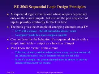
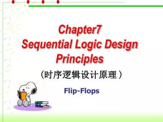
Chapter7 Sequential Logic Design Principles. ( 时序逻辑设计原理 ). Types of Logic Circuits. Combinational logic circuit Outputs depend only on the current values of the inputs No feedback loop, No Memory Device Sequential logic circuit Outputs depend on - the current values of the inputs

E N D
Chapter7 Sequential Logic Design Principles (时序逻辑设计原理)
Types of Logic Circuits • Combinational logic circuit • Outputs depend only on the current values of the inputs • No feedback loop, No Memory Device • Sequential logic circuit • Outputs depend on - the current values of the inputs - the past values of the inputs • Feedback loop, Memory Device
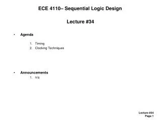
X0 Y0 X1 Y1 Xn Yn C1 C2 Ripple adder X Y CI CO S X Y CI CO S X Y CI CO S 0 C S0 S1 Sn X0 Y0 X2 Y2 X1 Y1 X Y CI CO S C2 C3 C0 C1 C1 C2 Feedback S0 S2 S1 Consider: Can we use one full adder to implement multi-bit ripple adder? — Feedback — clock control
X0 Y0 X1 Y1 Xn Yn C1 C2 Ripple adder X Y CI CO S X Y CI CO S X Y CI CO S 0 C S0 S1 Sn Xi Yi Clock X Y CI CO S Ci Ci+1 store Si Need Memory
Sequential Logic Circuit • Sequential Logic Circuit – Output depends on current and previous inputs – Hold/store previous information (i.e., state) – The state is a collection of state variables. – A circuit with n binary state variables has 2n possible states. – So sequential circuits are sometimes called Finite State Machine (FSM)
tH tL CLK tper We need a clock • The state changes of most sequential circuits occcur at times specified by a free-running clock signal. rising edge falling edge high level low level Period = tper Frequency=1/tper Duty cycle=tH/tper(or tL/tper )
Chapter Outline • Latches and Flip-Flops (锁存器和触发器 ) • Clocked Synchronous State-Machine Analysis (同步时序分析) • Clocked Synchronous State-Machine Design (同步时序设计)
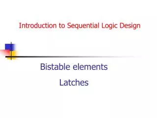
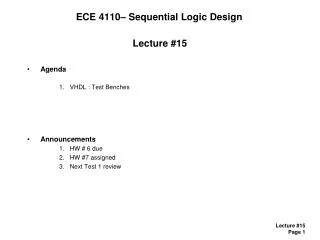
Q Q_L Q Q_L 7.1 Bistable Elements (双稳态元件) 1 0 0 1 1 0 0 1 • Two Stable State: Q = 1 ( HIGH , 1态) and Q = 0 ( LOW , 0态) —— Bistable Circuit(双稳电路) • When Power is first Applied to the circuit, it Randomly Comes up in One State or the Other and Stays there Forever.
Stable 稳态 Vin1 Vout1 Vout1 Q = Vin2 Metastable 亚稳态 Q_L Vin2 Vout2 Vin1 Vin2 Vout2 = Vout2 Vout2 Vin2
Q Q_L Metastable Behavior(亚稳态特性) • Metastability is the situation where the inputs cause an indeterminate output in a feedback circuit • Random Noise will tend to Drive a circuit that is Operating at the Metastable Point to one of the Stable operating point. ( 随机噪声会驱动工作于亚稳态点的电路转移到一个稳态的工作点上去 )
Stable Stable Metastable Behavior(亚稳态特性) • Apply a definite Pulse Width from a Stable state to the Other. (从一个“稳态”转换到另一个“稳态”需加一定宽度的脉冲(足够的驱动)) Metastable • All sequential circuits are susceptible to metastable behavior.
7.2 Latches and Flip-Flops(锁存器与触发器) • The Basic Building Blocks of most Sequential Circuits. • Latches(锁存器) • A sequential device watches its inputs continuously and can change its outputs at any time • In some cases requiring an enable signal to be asserted. • Flip-Flops( F/F,触发器) • A sequential device samples its inputs and changes its outputs only when a clocking signal is changing.
0 R Q QN S 0 Q NOR NOT QN S-R Latches Function Behaviors: (1)S = R = 0 Keep the last state 电路维持原态 Qn+1 = Qn QNn+1 = QNn 新 态 原 态
1 1 R Q (a) 1 QN S 0 0 0 0 R Q 0 1 (b) 0 1 0 QN S S-R Latches Reset Function Behaviors: 0 (2)S = 0, R = 1 锁存器清0:Qn+1=0 QNn+1=1 即使S,R无效(=0) 锁存器仍能锁定0态 1 a. 原态:Qn=0,QNn=1 新态:Qn+1=0,QNn+1=1 b. 原态:Qn=1,QNn=0 新态:Qn+1=0,QNn+1=1 1
0 0 R Q (a) 0 QN 1 S 1 1 0 R Q 1 0 (b) 0 1 0 QN S S-R Latches Set Function Behaviors: 1 (3)S = 1, R = 0 锁存器置1:Qn+1=1 QNn+1=0 即使S,R无效(=0) 锁存器仍能锁定1态 0 a. 原态:Qn=1,QNn=0 1 新态:Qn+1=1,QNn+1=0 b. 原态:Qn=0,QNn=1 新态:Qn+1=1,QNn+1=0
1 R 0 Q “禁止” QN S 0 1 0 Q QN 0 S-R Latches Function Behaviors: (4)S = R = 1 Qn+1 = QNn+1 = 0 When S,R are both negated(=0) 亚稳态,对噪声敏感 状态不确定
The time delay in S-R latch Initial state: Q=0 Last state: Q=1
t=0 S=0 R=0 If input from 11 to 00 Initial state: Q=0 QN=0 Last state: Q=? QN=? Metastable • Try to hold an unstable state
t=38 Q=1 QN=1 t=57 Q=0 QN=0 t=76 Q=1 QN=1 If input signal is too short Initial state: Q=0 Last state : metastable
Summery of S-R latch SR = 01 set 0 ; SR = 10 set 1 ; SR = 00 hold : hold the state ; Try to hold an unstable state : metastable Minimum-pulse-width tpw(min) : minimal set time to avoid metastable !
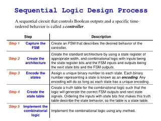
State transition table Reset R Q S R Qn Qn+1 0 0 0 0 0 1 0 1 0 0 1 1 1 0 0 1 0 1 1 1 0 1 1 1 0 1 0 0 1 1 0* 0* QL Set S S R Q QL 0 0 0 1 1 0 1 1 维持原态 0 1 1 0 0* 0* S Q R QL S Q R Q S-R Latches Function Table Logic Symbol
State transition table Qn+1 SR S R Qn 00 01 11 10 Qn+1 Qn 0 0 0 0 0 1 0 1 0 0 1 1 1 0 0 1 0 1 1 1 0 1 1 1 0 1 0 1 0 0 1 1 0* 0* 0 0 1 1 0 1 特征 方程 S=1,R=0 S=X R=0 S=0 R=X 0 1 S=0,R=1 Qn+1 = S + R’·Qn S·R = 0 约束条件 State diagram
S S R Q QN R 0 0 0 1 1 0 1 1 维持原态 0 1 1 0 0* 0* Q QN S R Q tpw(min) tpLH(SQ) tpHL(RQ) 最小脉冲宽度 传播延迟
S-R锁存器功能表 S_L Q S_L R_L Q QL 1 1 1 0 0 1 0 0 维持原态 0 1 1 0 1* 1* QL R_L 逻辑符号 S Q R Q S’-R’ latch S’ 清0 置1 不定 R’ 电路维持原态 S_L = R_L = 1 S_L = 1, R_L = 0 Q = 0, QL = 1 S_L = 0, R_L = 1 Q = 1, QL = 0 S_L = R_L = 0 Q=QL=1,不定状态
S_L S 功能表 Q C S R Q QL C 维持原态 维持原态 0 1 1 0 1* 1* 0 X X 1 0 0 1 0 1 1 1 0 1 1 1 QL R R_L 逻 辑 符 号 S C R Q Q S-R Latch with Enable —— 又称“时钟S-R锁存器” (1). C = 0时: 维持原态 (2). C = 1时: 与S-R锁存器相似 注意:当S=R=1时,若C由10, 则下一状态不可预测。
C S R Q QL 0 X X 1 0 0 1 0 1 1 1 0 1 1 1 维持原态 维持原态 0 1 1 0 1* 1* C S R Q Typical operation of an S-R latch with enable
S D Q C QL Dlatch function table R C D Q QL 1 0 0 1 1 1 1 0 0 X 保持 Logic symbol D Q C Q Q = D D Latch Data input Control input ENABLE CLK 输出状态保持不变 C = 0, 输出随输入状态而改变 C = 1, D = 1时,Q = 1 D = 0时,Q = 0 The state is decided by the input Directly ! Transparent Latch (透明锁存器)
State transition table D Qn+1 0 1 0 1 D=1 D=1 D=0 0 1 D=0 Function Description of a D Latch Characteristic equation: Qn+1 = D(C=1) State diagram
C D Q tpLH(CQ) tpLH(DQ) tsetup thold tpHL(DQ) tpHL(CQ) 建立时间 setup time 保持时间 hold time Timing Parameters for a D Latch • Setup time(建立时间,输入信号先于时钟到达的时间) • Hold time(保持时间,有效时钟沿后输入信号保持的时间) 在C的下降沿附近有一个时间窗 这段时间内D输入一定不能变化
S-R latch with enable The input pulse may be cut off by control signal ! Hold time: after the change of C 0→1 ;Setup time: before the change of C 1→0 .
D Q C Q D Q C Q D Q C Q D Q C Q DIN[3:0] WR RD DOUT[3:0] Applications of Latches
Xi Yi Ci X Y CI S CO Si Ci+1 Xi Yi 时钟控制 X Y CI CO S Ci Ci+1 Q D Q C Si Applicationsof Latches 串行输入、串行输出 注意:时钟同步 CLK 再谈串行输入 加法器的实现 暂存
7.4 7.5 Homework