Download
1 / 19
190 likes | 197 Views
TDC L0 Buffer. L1 Buffer. DAQ. ASD. ~100m. 50 fC. bias. L0 BX. L1. chamber. counting room. Ulrich Uwer University of Heidelberg. LHCC Review CERN, 27/01/2003. Outer Tracker Electronics. TFC ECS. HV. L1. LV. GOL. LV Reg. OTIS. OTIS. ASDBLR. ASDBLR. ASDBLR. HV board.

E N D
TDC L0 Buffer L1 Buffer DAQ ASD ~100m 50 fC bias L0 BX L1 chamber counting room Ulrich Uwer University of Heidelberg LHCC Review CERN, 27/01/2003 Outer Tracker Electronics
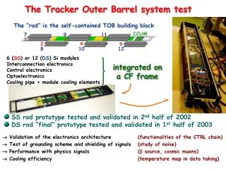
TFC ECS HV L1 LV GOL LV Reg OTIS OTIS ASDBLR ASDBLR ASDBLR HV board tot. dose < 10krad ASDBLR Module End: 128 channels 16 ASDBLR chips 4 OTIS TDC chips 1 optical link: 1.28 Gbit/s Outer Tracker: ST1…3 56000 channels 432 optical links
X 1 GOL/Aux Board • Front-end cards: • have to fit inside a closed metal shielding box: 22 x 30 x 4 cm • excellent ground connection to straw-tubes and module reference ground • power dissipation of cards is about 22 W / box → water cooling • easy access should be maintained TDC boards X 2 ASD boards HV boards X 4 X 8
Front-end electronics box: How it fits together cooling bar cooling plates and blocks plates of shielding box module support bar Feed-through board
HV Boards eventual. used as fuse R=560kΩ C=330pF Z=300Ω Z=300Ω1) Capacitors: JOHANSON 302R29W331KV4E Max. Volt.: 4kV Size: 4.6 x 2 x 1.5 mm3 32 channels per board Capacitors embedded in PCB: 1)Z=150Ω at high frequencies + 150Ω in series
Long term tests: • 19 boards = 608 channels • HV = +2.5 KV, t = 14 days • → I (32 cha) < 50 nA • → 1 failing cap Humidity: 45% 2. Temperature cycling: every hour 25-65oC HV = +2.5 KV, t = 14 days → 1 failing cap I (A) T=21oC More studies needed 14 days
TDC board: • radiation hard OTIS TDC chip • provides bias voltage for ASD • power rooting for ASDBLR card • test pulses for ASDBLR ASDBLR chip: ATLAS DMILL version 02 joining ATLAS chip order
GOL / Auxiliary Board: Interface to outside voltage sensing optical Link TFC I2C power QPLL Clk Trg Rst TP I2C LV Data OTIS OTIS OTIS
OTIS TDC Chip Components: • 32 maskable channels • DLL, HitRegister, PrePipeline: 6 bit drift time encoding: 1 bit ↔ 0.39 ns (req. resolut. < 1ns) playback data feed-in (testing) • Pipeline, Derandomizing Buffer: buffer length: 160 evts ↔ 4.0 μs • Control Algorithm: Memory and trigger management, 2 read-out modes: 1, 2, 3 BX/evt • I2C Slow Control Interface: Programming, ASD bias setting • DAC: ASD-Chip bias 0.25 μm CMOS technology
OTIS Readout Modes Problem: max. drift-time 42 ns → min. 2 BX / evt • All hits of n BX with possible truncation for length > 36 bytes: • → variable event length • II. Single (first) hit mode • → fixed event length • preferred readout mode 320 Mbit/s @ 1.1 MHz L0
OTIS1.0 Prototype • First prototype with basic functionality • ~700.000 transistors • 5100µm x 6000µm • Submission: 15/04/2002 Delivery: 29/07/2002 • Small test PCB: possibility to connect ASD and GOL chips
OTIS1.0 Status DLL test chip good progress
Drift time measurement: • In 2nd half of BX clock times are not correctly encoded: studies (measurements and simu-lation) revealed timing problems between data bits and Clk signal at memory input reason : parasitic capacities • Double hit measurement: 1st hit to pre-charge
OTIS Time Schedule 2003 2004 2005 03/03 OTIS chip review MPW11: Submission OTIS1.1 07/03 Validation of OTIS baseline Delivery of OTIS1.1 – Start of test 10/04 OTIS 1.2 Engineering Run 01/05 Delivery of OTIS1.2 03/05 Start Electr Prod
Module Module Module 32 bits 32 bits 32 bits GOL GOL GOL OTIS OTIS OTIS From OTIS to L1 Buffer 1.28 (1.6) Gbits/s 1 2 3 4 5 6 7 8 9 101112 L1 Buffer PreProc for L1 Trig Trigger L1 Buffering and zero suppression DAQ <15 MB/s optical link • Total data volume: • 432 opt links → 36 L1 boards • total data flow at 40 KHz: 380 MB/s
Test bench for optical link VCSEL STRATOS optical transceiver GOL GOL Test board: GOL + VCSEL TI TLK2501 evaluation board Error rate < 10-13
L1 Buffer Board: Memory to accommodate L1 latency Common project Velo, IT, OT Outer Tracker
TFC: TTCrx + Rst Decoder → LVDS Signals → modules ECS: SPECS Slave → I2C bus lines → modules → JTAG → ADCs → LV sensing Low Voltage: passive +/- 5V distribution → modules High Voltage: passive distribution → 2 connections/modules Services: Service Box 1 service box / quadrant
Outer Tracker Electronics: Time Schedule 2003 2004 2005 07/03 Validation of OTIS baseline 10/03 Delivery of OTIS1.1 03/04 Start pre-series production 06/04 Pre-series finished: start mounting 01/05 Delivery of OTIS1.2 03/05 Start Mass Prod