Download
1 / 32
380 likes | 686 Views
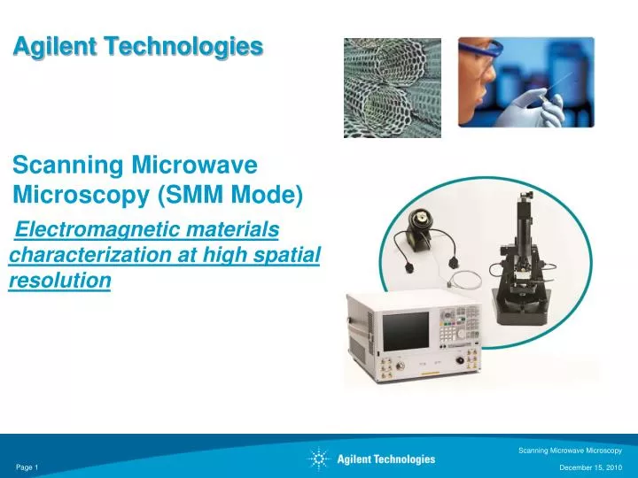
Agilent Technologies Scanning Microwave Microscopy (SMM Mode). Electromagnetic materials characterization at high spatial resolution . Overview . SMM System – PNA with AFM Features and Benefits Microwave Network Analyzer Basics (VNA) System overview

E N D
Agilent TechnologiesScanning Microwave Microscopy (SMM Mode) Electromagnetic materials characterization at high spatial resolution Scanning Microwave Microscopy
Overview • SMM System – PNA with AFM • Features and Benefits • Microwave Network Analyzer Basics (VNA) • System overview • Calibrated capacitance & dopant density • Beyond SCM, what can be done with SMM - Applications • Biological samples • Thin films and coatings • Quantum dots/quantum structures • Summary Scanning Microwave Microscopy
Features & Benefits • Provides exceptionally high spatial electrical resolution • Offers highest sensitivity and dynamic range in the industry • SMM facilitates • Complex impedance (resistance and reactance) • Calibrated capacitance • Calibrated dopant density • Topography measurements • Works on ALL semiconductors Si, Ge, III-V and II-VI • Does not require and oxide layer • Operates at multiple frequencies (variable up to 18GHz) Scanning Microwave Microscopy
Transmission S21 DUT S11 Reflection S22 S12 Magnitude RF Source Phase LO R2 R1 A B Test port 1 Test port 2 What is a Vector Network Analyzer? • Vector network analyzers (VNAs)… • Are stimulus-response test systems • Characterize forward and reverse reflection and transmission responses (S-parameters) of RF and microwave components • Quantify linear magnitude and phase • Are very fast for swept measurements • Provide the highest level of measurement accuracy Scanning Microwave Microscopy
A Reflected = R Incident High-Frequency Device Characterization Incident Transmitted R B Reflected A TRANSMISSION REFLECTION B Transmitted = R Incident Group Return SWR Gain / Loss Delay Loss Insertion S-Parameters Impedance, Admittance S-Parameters S11, S22 Phase Reflection Transmission S21, S12 Coefficient R+jX, G+jB Coefficient G, r T,t Scanning Microwave Microscopy
Scanning Microwave Microscopy (SMM) Basic Idea Actuator • Tip and sample form a capacitor Capacitance Measuring C yields er C = e0er A/d C ~ fF Capacitance bridges too slow Integration times of several seconds not practical for imaging Scanning Microwave Microscopy
System Overview Coaxial cable Network Analyzer Scanning AFM in X and Y and Z (closed loop) • Network analyzer sends an incident RF signal to the tip through the diplexer • RF signal is reflected from the tip and measured by the Analyzer • Magnitude & phase of the ratio between the incident & reflected are calculated • Apply a model to calculate the electrical properties • AFM scans and moves tip to specific locations to do point probing Scanning Microwave Microscopy
Compatible with Agilent 5420 & 5600LS AFM/SPM 5600LS AFM 5420 AFM Scanning Microwave Microscopy
Sub 7 nm Conductive tip development Pt/Ir Cantilever Agilent Precision Machining and Process Technologies to deliver RF/MW to the conductive tip Alumina Carrier Scanning Microwave Microscopy
Simultaneous Imaging of Topography, Capacitance, and dC/dV Scanning Microwave Microscopy
PNA Controls from PicoView Scanning Microwave Microscopy
Calibration staircase sample (collaboration with National Institute of Standards and Technology, NIST) Capacitance calibration C1 C2 10 micron Gold caps on SiO2 „staircase“ on Si. AFM topography 3D view (left) and schematic overview (right). Transfer Function: S11 signal [dB] capacitance [F] Scanning Microwave Microscopy
Capacitance Calibration C1 C2 Capacitance (amplitude) dB 16 12 8 4 0 10µm Sample: „NIST2“ staircase with goldcaps Scanning Microwave Microscopy
Capacitance Calibration Scanning Microwave Microscopy
Enhancing the Sensitivity • DPMM approach: • Use the Flatband transfer function as • AM mixer to modulate the reflected MW signal at the rate of drive frequency (<100 KHz). • The AM modulation amplitude is function of the dopant density. Scanning Microwave Microscopy
Imaging Dopant Density Agilent PNA AFM Wave-guide Source Coupler Coupler A B Scanner LO LO A/D Probetip A/D Sample LF Demodulator LF AC Bias dC/dV Module Agilent DPMM Scanning Microwave Microscopy
Spec sheet IMEC calibration sample bulk 2 edge Dopant Density calibration with IMEC Standard Resistivity [Ωcm] 1000 1 0.001 1014 1017 1020 Deposit Layers with Various Doping Levels 30 20 10 0 Depth [µm] Cleave or polish from top to expose the layers 4 1 Si Wafer Density (/cm³) 6 3 8 5 7 Scanning Microwave Microscopy
Dopant Density calibration with IMEC Standard dC/dV Amplitude edge bulk 1 2 3 4 5 6 7 8 Scanning Microwave Microscopy Page 18
Images of an SDRAM Topography dC/dV Capacitance Images of SDRAM chip acquired with SMM Mode. The underneath n-type (bright) and p-type doped structure clearly indentified in both capacitance and dC/dV Images (W.Han) • Very high sensitivity • Can see semiconductor, insulators and conductors • Can be calibrated • Can also get inductance and reactance Scanning Microwave Microscopy
SMM Images of SRAM Chip • Topography (A and C) and dC/dV (B and D) images of SRAM. C and D are zoomed scans on one of the transistors in the n well marked in the blue square in A / B. A very fine line feature of 10 to 20 nm in width can be seen in the dC/dV image, as pointed in D, indicating high resolution capability of the scanning microwave microscope. Scanning Microwave Microscopy
Simultaneous Images of SRAM Chip • Simultaneous topography (A), capacitance (B), and dC/dV (C) images of an SARM chip. Alternating lightly doped p and n wells are clearly identified in both capacitance and dC/dV images. Five of the six transistors in a unit cell are marked in B and C. Scanning Microwave Microscopy
Dopant on SiGe Topography (left) capacitance (middle) and dC/dV (right) images of a dpoed SiGe device acquired with Scanning Microwave Microscopy (SMM). Both capacitance and dC/dV images showed dopant structure not seen topography. Scanning Microwave Microscopy
InGaP/GaAs Transistor Topography (left) and impedance (right) images of a cross section of a InGaP/GaAs hetrrojunction bipolar transistor. Different regions from the emitter to the subcollector with different dopant levels were clearly resolved in the impedance image. (W. Han sample courtesy of T. Low) Scanning Microwave Microscopy
Semiconductor Failure Analysis Optical image of a small section of the tested SRAM chip. The failed bit contains an n-type FET (the 48th on that row) with an abnormal Vt. Four sets (A, B, C, and D) of scanning microwave microscopy images on the failed SRAM chip. Each set contains topography (top), dC/dV (middle), and VNA amplitude (bottom) images acquired simultaneously. The red squares outlined the failed 48th n-type FET, the blue squares are normal n FETs on the same row. Scanning Microwave Microscopy
Bacteria Cells Topography (left) and impedance (right) images of dried bacteria cells. (W. Han, Sample courtesy of N Hansmeier, T. Chau, R.Ros and S. Lindsay at ASU) Scanning Microwave Microscopy
Summary • Characterization of electromagnetic materials at High spatial resolution • Offers highest sensitivity and dynamic range in the industry • Complex impedance • Sidewall diffusion • Calibrated capacitance – unique • Calibrated dopant density – unique • Works on ALL semiconductors Si, Ge, III-V and II-VI • Does not require and oxide layer • Operates at multiple frequencies (variable up to 18GHz) Scanning Microwave Microscopy
Back-up Slides Scanning Microwave Microscopy Scanning Microwave Microscopy
Scanning only • qualitative • poor sensitivity • limited 1015-1020 Atoms/cm3 • No Conductors/Insulators Scanning Microwave Microscopy
Lightwave Analogy to RF Energy Incident Transmitted Reflected Lightwave DUT RF Scanning Microwave Microscopy
Standard Vector Network Analyzeras a reflectometer Very small capacitor High SNR Low Resolution Source A B LO LO A/D A/D Probe Highly resistive load High SNR Low Resolution Load close to 50 Ohms Low SNR High Resolution Figure 1: reflection coefficient vs.. impedance Low resistive load High SNR Low Resolution Scanning Microwave Microscopy
Simplified Single Frequency Solution Source A B 50 Ohm Half wave length Coaxial resonator LO LO A/D A/D Probe Scanning Microwave Microscopy