Download
1 / 1
10 likes | 147 Views
4th International Conference on Materials for Advanced Technologies, Singapore July 1-6, 2007. Novel Multiple-Valued Memory Design by Standard SiGe Process. Kun Shan University. Department of Electronic Engineering. Student : Yi-Jhih Lin. Advisor : Kwang-Jow Gan. Abstract

E N D
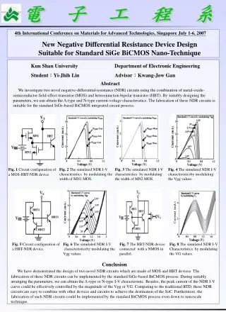
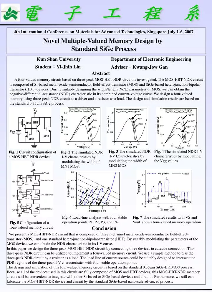
4th International Conference on Materials for Advanced Technologies, Singapore July 1-6, 2007 Novel Multiple-Valued Memory Design by Standard SiGe Process Kun Shan University Department of Electronic Engineering Student:Yi-Jhih Lin Advisor:Kwang-Jow Gan Abstract A four-valued memory circuit based on three-peak MOS-HBT-NDR circuit is investigated. The MOS-HBT-NDR circuit is composed of Si-based metal-oxide-semiconductor field-effect-transistor (MOS) and SiGe-based heterojunction-bipolar-transistor (HBT) devices. During suitably designing the width/length (W/L) parameters of MOS, we can obtain the negative-differential-resistance (NDR) characteristic in its combined current-voltage curve. We design a four-valued memory using three-peak NDR circuit as a driver and a resistor as a load. The design and simulation results are based on the standard 0.35μm SiGe process. Fig. 3 The simulated NDR I-V Characteristics by modulating the width of MN2 MOS. Fig. 4 The simulated NDR I-V characteristics by modulating the Vgg values. Fig. 1 Circuit configuration of a MOS-HBT-NDR device. Fig. 2 The simulated NDR I-V characteristics by modulating the width of MN1 MOS. Fig. 6 Load-line analysis with four stable operation points P1, P2, P3, and P4. Fig. 7 The simulated results with VS and Vout shows four-valued memory operation. Fig. 5 Configuration of a four-valued memory circuit Conclusion We present a MOS-HBT-NDR circuit that is composed of three n-channel metal-oxide-semiconductor field-effect-transistor (MOS), and one standard heterojunction-bipolar-transistor (HBT). By suitably modulating the parameters of the MOS device, we can obtain the NDR characteristic in its I-V curve. In this paper we design the three-peak MOS-HBT-NDR circuit by connecting three devices in cascade connection. This three-peak NDR circuit can be utilized to implement a four-valued memory circuit. We use a simple method to bias the three-peak NDR circuit by a resistor as a load. The load line of current source could be suitably designed to intersect the PDR regions of the three-peak I-V characteristics with four stable operation points. The design and simulation of this four-valued memory circuit is based on the standard 0.35μm SiGe-BiCMOS process. Because all of the devices used in this circuit are fully composed of MOS and HBT devices, this MOS-HBT-NDR memory circuit will be convenient to integrate with other Si-based or SiGe-based devices and circuits. Furthermore, we still can fabricate the MOS-HBT-NDR device and circuit by the standard SiGe-based nanoscale advanced process.