Download
1 / 20
220 likes | 363 Views
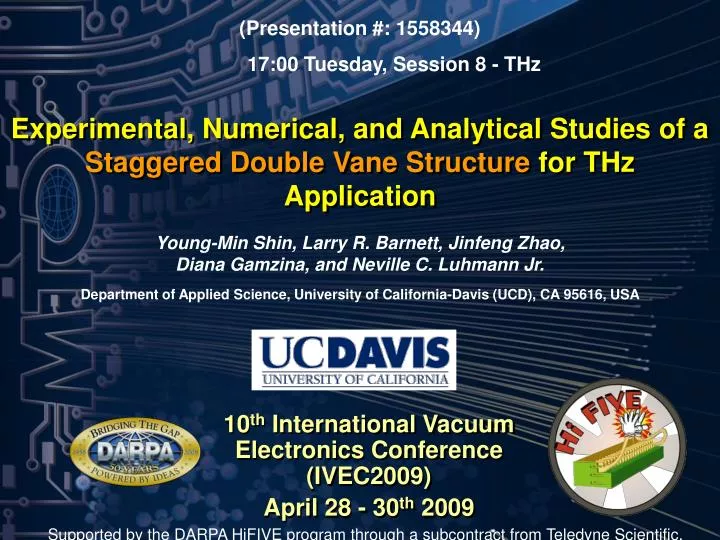
(Presentation #: 1558344) . 17:00 Tuesday, Session 8 - THz . Experimental, Numerical, and Analytical Studies of a Staggered Double Vane Structure for THz Application. Young-Min Shin, Larry R. Barnett, Jinfeng Zhao, Diana Gamzina, and Neville C. Luhmann Jr.

E N D
(Presentation #: 1558344) 17:00 Tuesday, Session 8 - THz Experimental, Numerical, and Analytical Studies of a Staggered Double Vane Structure for THz Application Young-Min Shin, Larry R. Barnett, Jinfeng Zhao, Diana Gamzina, and Neville C. Luhmann Jr. Department of Applied Science, University of California-Davis (UCD), CA 95616, USA 10th International Vacuum Electronics Conference (IVEC2009) April 28 - 30th 2009 Supported by the DARPA HiFIVE program through a subcontract from Teledyne Scientific.
Overview Motivation and Goal Cathode and Electron Gun Circuit Design and Analysis Interaction Circuit Fabrication - KMPR UV LIGA - High Precision CNC Machining Cold-Test Setup Summary and Future Plans
220 GHz Sheet Beam TWT • MEMS-Integrated High Power Vacuum Amplifier for THz Communication and Sensing Systems • - Vacuum Electronic Circuit Elements • High current density, long-life cathode (UCD and Teledyne Scientific) Tungsten-ScandateNanopowder cathodes capable of 80 A/cm2 • High aspect-ratio electron beam (CPI and Teledyne-MEC) Elliptical cathode with beam compression produces 7:1 aspect ratio beam for SBTWT, 25:1 aspect ratio beam for beam-stick • High efficiency interaction structure (UCD and Teledyne Scientific) Novel staggered vane interaction structure at 220 GHz shows 50 GHz bandwidth, 13 dB/cm gain, and 100 W output • High power MMIC driver (Teledyne Scientific and UCSB) InP based solid state amplifier 50 mW output at 220 GHz • High efficiency thermal management (Teledyne Scientific) Integrated cooling channels around MEMS interaction structure
Nano-Composite Cathode • Scandate Nano-Composite (Sc2O3-W) Cathode See Zhao et al., Session 23 - Cathodes II After Furnace Sinter: Grain size in matrix is 272 nm and very uniform EDX Analysis on the SpectraMat 311X Surface Sol-gel Method • Current Density versus Cathode Button Voltage UCD Cathode: 80A/cm2 fully space charge limited • 1150oC for 800 hrs (33 days)
Cathode Testing at UC Davis High Current Density Operation of Spectra-Mat: 311X UC Davis Cathode • At 1272 °Cb the emission at 50 A/cm2 is • still only about 70% SCL • Even at 30 A/cm2 it takes at least • 1250 °Cbto reach ~90% SCL
Cathode Testing at UC Davis Cathode Testing New High Perveance Cathode Life Test Vehicle Multiple rapid cathode life test facility Rapid button test System operational Cathode testing and life testing underway at UC Davis: eight vehicles operational with another four nearing completion G. Scheitrum and A. Hasse Three 3.0 P CLTVs completed
Machined WSBK Circuit Overview of Interaction Structure Approach: Staggered double vane structure provides large bandwidth and good coupling to sheet electron beam Circuit Dimensions: Beam Tunnel (b x h) 770 x 150 µm Vane Period (d) 460 µm Vane Height (L) 270 µm Vane Thickness (d-a) 115 µm Vane Width (h) 770 µm Beam Size: 700 μm × 100 μm (7 : 1), 400 A/cm2
Overview of Interaction Structure Comparison of double vane structures
Circuit Design and Analysis • 3D Model • Dispersion and Transmission Graphs • Operating Conditions • Beam Voltage (Ve)= 20 kV • Beam current (Ie) = 0.25 A • Center frequency (fc) = 220 GHz • Opt. phase-shift () = 2.5 (n = 1) • Transmission Loss : • ~ - 0.6dB (avg.) • Attenuation: ~ 0.15dB/cm (avg.) • Dimensional Parameters • L = 270 m • h = 770 m • b = 150 m • d = 460 m • MAGIC3D PIC Simulation Analysis 150 ~ 275W • Bandwidth (Cold) ~ 70 GHz (30%) 1) Larry R. Barnett and Young-Min Shin, US Patent Application No. 60979392, Oct. 12 (2007) 2) Young-Min Shin and Larry R. Barnett, Appl. Phys. Lett. 92, 091501 (2008). 3) Young-Min Shin, Larry R. Barnett, and Neville C. Luhmann Jr., Appl. Phys. Lett. 93, 221503 (2008) 4) Young-Min Shin, Larry R. Barnett, and Neville C. Luhmann Jr., IEEE Trans. Elec. Dev. (in press), (May. 2009) * Larry R. Barnett and Young-Min Shin, US Patent Application No. 60979392, Oct. 12 (2007)
Broadband Coupler • Tapered Transition (Vane Width) • Ka-band circuits
MAGIC3D: Gain and Stability Growth Rate ~ 14dB/cm 30dB
Sensitivity Studies • Misalignment Effect y y z z dy dz x x • Off-Centered Beam Effect
KMPR UV LIGA Process • MEMS Facility • UV-LIGA • Northern California Nanotechnology Center (NCNC) @ UCD
Non-Uniform Resist Thickness UV LIGA Technical Issues • Heavy table that can absorb vibrations and can be leveled • Stone hotplate with low thermal expansion coefficient that can also be leveled accurately • Lapped and polished copper substrate with thickness deviation of less than 1 µm over the circuit area • Underexposure Results: Film Thickness Uniformity Improvement Over the 4” wafer : 5 m Over the circuit area (25 × 25 mm) : ~1 - 2 m Lapped and polished to within 0.25 µm Less than 1 µm undercut after mold removal • Overexposure wrinkles
Surface Roughness Analysis of Resistivity versus S21 and S11 • Transmission (S21) Graph • 10 mm long BS circuit model • Resistivity versus S21/S11 • Reflection (S11) Graph Only 1 dB in S21 and S11 is changed by up to 5 × Resistivity (OHFC) Interaction circuit is insensitive to surface conditions (roughness)
θ Sensitivity Analysis of Fabrication Errors • Sidewall Slope versus Frequency Deviation Sidewall Slope (> 2) Frequency Deviation (> 2 %) Vertical sidewall of less than 2 can be controlled by common photo-lithography process. • Undercut versus Frequency Deviation Undercut ( 40 m) Frequency Deviation ( 2 %) Undercut size of UV LIGA mold is much smaller : ~ 10 – 20 m
Process Optimization • System Setup for Process Optimization • Before Softbake • Right After Heating • After 4.5 hr Softbake • Large Hotplate • (Rapid Production) • Autocollimator • (Leveling) • Copper Substrate Flatness Analysis * 1 fringe = 0.25 m 6 wafers/cycle Thickness Uniformity : 1 m over the circuit (25 mm) • UV Lithography • Mold Removal Dimensional accuracy : 3 m, sidewall slope: 90 ± 2 Mold removal efficiency: 90 %
Completed Circuit and Analysis • UV LIGA Fabricated BS Circuit • Line Resolution and Surface Roughness • Line Resolution Pattern Images • AFM-Measured Surface Roughness Surface Roughness ~ 50 - 100 m Aspect ratio ~ 10 : 1 Young-Min Shin, Diana Gamzina, Larry R. Barnett, and Neville C. Luhmann Jr. “UV Lithography and Molding Fabrication of Ultra-Thick Micrometallic Structure using a KMPR Photoresist ”, IEEE J. Microelec. Micro. Sys. (MEMS) (submitted, 2009)
220GHz (~0.14 µm) (2) • LIGA-(Cu) : 70 nm • DRIE-(plated Si) : 100 nm • LIGA-(PMMA Mold) : 20 nm (3) Required Surface Roughness • Frequency versus Required Skin Depth for Device Operation
Summary and Future Plans Accomplishments Sc2O3-W Nano-Powder Cathode A. Maximum Emission Current Density: ~ 80 A/cm2 at 1150 oC (Full Space Charge Limited) B. Life-Time: 768 hrs (950 oC), 800 hrs (1150 oC) C. ~ 50 A/cm2 at 1050 oC Sheet Beam Gun Design (CPI and Teledyne-MEC) Circuit Design and Analysis A. Operational Bandwidth : 70 GHz (30%) @ 220 GHz B. Output Coupling Bandwidth: 66 GHz (88%) C. MAGIC3D Simulation: Power Growth Rate (14 dB/cm), Max. Efficiency (5%) MEMS Fabrication A. UV LIGA : Critical Dimensions ( 5 m), Surface Roughness (~ 50-100 nm), Aspect Ratio (~ 10 : 1) CNC Fabrication • Research Schedule • 750 A/cm2 and 25 : 1 Sheet Beam Transport Test • 220 GHz Circuit Cold-Test