Download
1 / 34
360 likes | 496 Views
Timing Behavior of Gates. Gates Have Non-Linear Input/Output Behavior. V cc. V out. 0V. V cc. V in. Plotting V out vs. V in shows non-linear voltage behavior. Gates Also Don’t React Immediately. V in. V out. t prop-rise. V in. t prop-fall. V out. t fall. t rise. time.

E N D
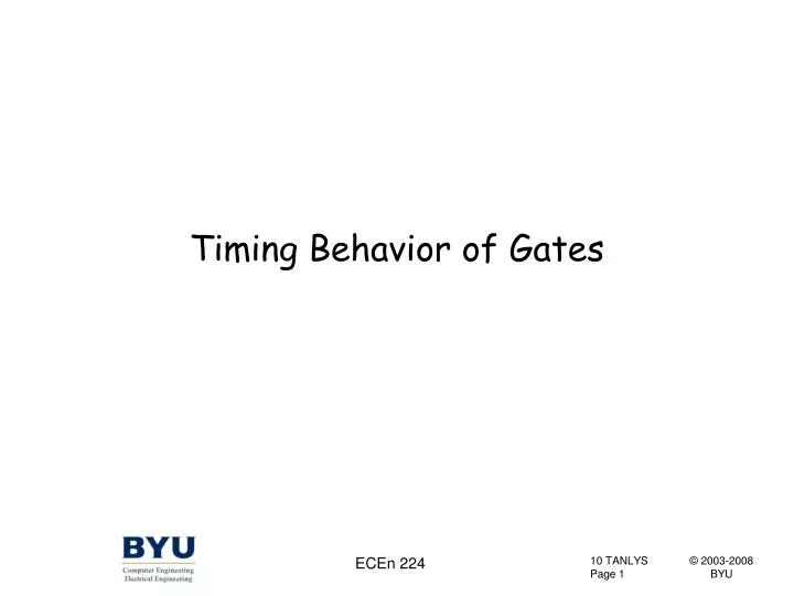
Timing Behavior of Gates ECEn 224
Gates Have Non-Linear Input/Output Behavior Vcc Vout 0V Vcc Vin Plotting Vout vs. Vin shows non-linear voltage behavior ECEn 224
Gates Also Don’t React Immediately Vin Vout tprop-rise Vin tprop-fall Vout tfall trise time tprop-fall and tprop-rise are measured from 50% of input swing to 50% of output swing trise is measured from 10% of output swing to 90% of output swing tfall is measured from 90% of output swing to 10% of output swing ECEn 224
Kinds of Gate Delays • Propagation Delays • Match intuition about how fast the gate is… • Rising and falling delays may be different • Take into account which nodes rising, which nodes falling to compute delay through network • Rising and falling delays may be the same • Ignore rising/falling behavior • Will use most of this semester • Rise and Fall Times • Only indirectly related to how fast the gate is… • Values depend on what is being driven • Will not use in this course ECEn 224
Gate Delays • Delay values are usually provided for the gates you use • Use those delay values when analyzing a circuit’s timing • Here are the timing values we will use in this chapter • Wider gates are slower • AND = NAND+NOT, etc… ECEn 224
Critical Path Analysis • Given a logic circuit, how fast will it run? • How fast will its output react to changes on its inputs? • Find the slowest path from any input to the output • That is the critical path • Add up propagation delays along that path F A A B B F G E C C D D Delay = tOR2 + tAND2 = 7 ns Delay = 2 x tNAND2 + tOR3 = 10 ns ECEn 224
Kinds of Timing Analysis • The more detail you provide the more accurate the result • Separate tprop-rise and tprop-fall more accurate than a single tprop • Take into account other effects more accurate • Temperature • Power supply voltage • Manufacturing variation • Rise/fall times ECEn 224
Environmental Delay Effects • Temperature Variation • Chips run faster when cool, slower when hot • Voltage Variation • Value of Vcc can affect delay • Manufacturing Variation • Two gates on the same integrated circuit may run at slightly different speeds • Summary: gate delays are usually given as a maximum or a range of values that operational delay is guaranteed to be within. • Example: 2 ns +/-0.2 ns ECEn 224
Loading Effects • A gate that drives more circuitry is slower than a gate that drives less circuitry • When a signal drives multiple inputs, called fanout D C A E B Less heavily loaded faster More heavily loaded slower F ECEn 224
Typical Loading-Dependent Delay • Typical delay = tprop + k x Cload Load Loading-independent delay Loading-dependent factor For MOS technology, load is mostly capacitance For bipolar technology, load is both capacitance and current ECEn 224
Analyzing A Logic Network C=1 G A B=1 F tNAND2 tNAND2 A F G ECEn 224
A E B=1 G C=1 D F More Analysis 5ns 32ns A B 5ns 32ns A•B 8ns 35ns E C 20ns 30ns D 20ns 30ns C•D 23ns 33ns F 8ns 23ns 33ns 35ns E+F 12ns 27ns 37ns 39ns G ECEn 224
A E B=1 G C=1 D F More Analysis 5ns 32ns A B 5ns 32ns A•B 8ns 35ns E C 20ns 30ns D 20ns 30ns C•D 23ns 33ns F 8ns 23ns 33ns 35ns E+F 12ns 27ns 37ns 39ns G ECEn 224
A E B=1 G C=1 D F More Analysis 5ns 32ns A B 5ns 32ns A•B 8ns 35ns E C 20ns 30ns D 20ns 30ns C•D 23ns 33ns F 8ns 23ns 33ns 35ns E+F 12ns 27ns 37ns 39ns G ECEn 224
A E B=1 G C=1 D F More Analysis 5ns 32ns A B 5ns 32ns A•B 8ns 35ns E C 20ns 30ns D 20ns 30ns C•D 23ns 33ns F 8ns 23ns 33ns 35ns E+F 12ns 27ns 37ns 39ns G ECEn 224
A E B=1 G C=1 D F More Analysis 5ns 32ns A B 5ns 32ns A•B 8ns 35ns E C 20ns 30ns D 20ns 30ns C•D 23ns 33ns F 8ns 23ns 33ns 35ns E+F 12ns 27ns 37ns 39ns G ECEn 224
A E B=1 G C=1 D F More Analysis 5ns 32ns A B 5ns 32ns A•B 8ns 35ns E C 20ns 30ns D 20ns 30ns C•D 23ns 33ns F 8ns 23ns 33ns 35ns E+F 12ns 27ns 37ns 39ns G ECEn 224
A E B=1 G C=1 D F More Analysis 5ns 32ns A B 5ns 32ns A•B 8ns 35ns E C 20ns 30ns D 20ns 30ns C•D 23ns 33ns F 8ns 23ns 33ns 35ns E+F 12ns 27ns 37ns 39ns G ECEn 224
Completing a Timing Diagram – A Method • Do most upstream signals first • A and D in previous picture • For every instant in timing diagram • Compute each gate output as function of input(s) • Place new gate output after appropriate delay on timing diagram. • Move to downstream signals ECEn 224
Completing a Timing Diagram – A Shortcut Method • Focus on input changes (edges) • Everything constant in between ECEn 224
A F B Glitch Behavior • Does the glitch propagate to the AND output? A B F ? ECEn 224
A F B A B F Behavior #1 • Called transport delay • All glitches, no matter how narrow are propagated to output ECEn 224
A F B Behavior #2 • Called inertial delay • Glitches narrower than some threshold are filtered out A B F ECEn 224
Which Behavior Is Correct? • Wires usually exhibit transport delay • Gates usually exhibit some form of inertial delay • Regardless, both wires and gates will filter out (or change the waveform shape of) extremely narrow pulses • We will use transport for both gates and wires since we don’t know the pulse width thresholds ECEn 224
A Pulse Generator • F = A•A’ = 0 so why the pulse? • Due to gate delays A F A F Pulse width = 3 x tNOT ECEn 224
More Dynamic Gate Behavior F • What will this circuit do? • It will oscillate (0 – 1 – 0 – 1 - …) F Pulse width = tNOT Period of oscillation is 2 x tNOT ECEn 224
A’ B F A C Logic Hazards F = A’B + AC This is the conventional K-map solution ECEn 224
g1 A B=1 F g2 C=1 Called a hazard or false output: static equations indicate F=1 butdynamic behavior gives a “glitch” Gates Have Real Timing… A g1 Need to take into accounttiming of this inverter … g2 F ECEn 224
A B=1 F C=1 Hazards • Each prime implicant from K-map is implemented using a single AND gate • When moving between implicants, gates turn off and on at different times • Momentarily get false outputs ECEn 224
Hazard-Free Logic Design • Make sure all prime implicants overlap A’ g1 B g2 F A C Redundant butwill eliminatefalse output B g3 C F = A’B + AC + BC On ABC = ‘111’ to ABC = ‘011’, g3 will hold F high entire time. ECEn 224
A’ g1 B=1 g2 F A C=1 B=1 g3 C=1 No False Output… A g1 g2 g3 g3 holds F high whole time… F ECEn 224
Another Example Rule: No 2 adjacent 1’s should be in different implicants F = CD + AC’ F = CD + AC’ + AD This is not hazard-free This is hazard-free ECEn 224
When To Do Hazard-Free Design? • Do you always need to do HFD? • No… • Do it when you need to generate a signal that will not have glitches • Interfacing with other circuitry which is sensitive to edges • Asynchronous circuits ECEn 224
A Caveat • Method shown will only work for single-input changes • Other techniques for multiple-input changes ECEn 224