Download
1 / 12
160 likes | 203 Views
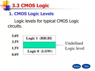
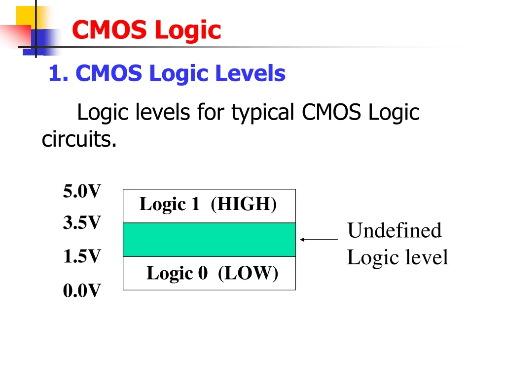
5.0V. Logic 1 (HIGH). 3.5V. Undefined Logic level. 1.5V. Logic 0 (LOW). 0.0V. CMOS Logic. 1. CMOS Logic Levels. Logic levels for typical CMOS Logic circuits. V IN. CMOS Logic. 2. MOS Transistors.

E N D
5.0V Logic 1 (HIGH) 3.5V Undefined Logic level 1.5V Logic 0 (LOW) 0.0V CMOS Logic 1. CMOS Logic Levels Logic levels for typical CMOS Logic circuits.
VIN CMOS Logic 2. MOS Transistors • A MOS transistor can be modeled as a 3-terminal device that acts like a voltage controlled resistance. • In digital logic applications, a MOS transistor is operated so its resistance is always either very high (and the transistor is “off”) or very low (and the transistor is “on”) .
drain gate + Vgs source - drain gate + Vgs source - CMOS Logic • n-channel MOS (NMOS) Increase Vgs→decrease Rds Normally, Vgs≥ 0 • Vgs=0 → Rds106 () • → I 10-6 (A) 0 • Vgs Vgs(th) → Rds 10 () << RL →VRds 0
source - Vgs + gate drain source - Vgs + gate drain CMOS Logic • p-channel MOS (PMOS) Decrease Vgs→decrease Rds Normally, Vgs 0 • Vgs=0 → Rds ≥ 106 () • Vgs Vgs(th) → Rds 10 () Switch Model Back
VDD=+5.0V VDD=+5.0V Q2 (PMOS) VOUT=H VIN=L VOUT VIN Q1 (NMOS) VDD=+5.0V VIN Q1 Q2 VOUT VOUT=L VIN=H 0.0(L) off on 5.0(H) CMOS Logic 3. Basic CMOS Inverter Circuit 5.0(H) on off 0.0(L) Back
VDD=+5.0V Q2 (PMOS) Z A Q1 (NMOS) CMOS Logic • CMOS inverter logical operation Truth table for CMOS inverter On when Vin is low. On when Vin is high.
VDD VDD VDD VDD VDD Z=H A=L Z=H Q2 Z=H Q4 A=L Z=L A=H B=L A=H B=H Z B=L B=H A Q1 B Q3 A Z B 3.3CMOS Logic 4. CMOS NAND Gates
VDD Q2 A B Q4 Z Q1 Q3 A Z B CMOS Logic 5. CMOS NOR Gates
VDD Q2 Q6 Q4 Z A Q1 B Q3 C Q5 CMOS Logic 6. Fan-In In principle, you could design a CMOS NAND or NOR gate with a large number of inputs. A 3-input CMOS NAND gate is showed in the figure. Why couldn't a CMOS gate has large number of inputs?
CMOS Logic 7. Noninverting Gates (P93) • AND Gate • OR Gate 8. CMOS AND-OR-INVERT Gate (P94) 9.CMOS OR-AND-INVERT Gate (P95)
Vcc VOHmin High-state DC noise margin HIGH 0.7Vcc VIHmin ABNORMAL VILmax 0.3Vcc Low-state DC noise margin LOW VOLmax 0 CMOS Logic • Logic Levels and Noise Margins • VOHmin: The minimum output voltage in the HIGH state. VOHmin=VCC–0.1V • VOLmax: The maximum output voltage in the LOW state. VOLmax=ground+0.1V
CMOS Logic • VIHmin: The minimum input voltage guaranteed to be recognized as a HIGH. VIHmin=0.7VCC • VILmax: The maximum input voltage guaranteed to be recognized as a LOW. VILmax=0.3VCC • DC noise margin: is a measure of how much noise it takes to corrupt a worst-case output voltage into a value that may not be recognized properly by an input. HIGH-state DC noise margin:VOHmin -VIHmin LOW-state DC noise margin: VILmax -VOLmax