Download
1 / 15
150 likes | 327 Views
FPGA (Field Programmable Gate Array). Presented By: Obaid ur Rehman Badar Hussain . FPGA. * A Field Programmable Gate Array (FPGA) is a Programmable Logic Device(PLD) with higher densities and capable of implementing different functions in a short period of time.

E N D
FPGA(Field Programmable Gate Array) Presented By: Obaid ur Rehman Badar Hussain
FPGA * A Field Programmable Gate Array (FPGA) is a Programmable Logic Device(PLD) with higher densities and capable of implementing different functions in a short period of time. * Topics covered:- • FPGA Overview • Logic Block • FPGA Routing Techniques • Programming Methodology • FPGA Design Flow
History Programmable Read Only Memory (PROM) • fuse programming • n- address i/p can implement n i/p logic fun. Problem: • Area efficiency. Programmable Logic Array (PLA) • Programmable AND plane followed by programmable or wired OR plane. • Sum of product form Problem : • Two level programming adds delay
Next Programmable Array Logic (PAL) • Programmable AND plane and fixed OR plane. • Flexible comparably. All these PLA and PAL are Simple Programmable Logic Devices (SPLD). Problem: • Logic plane structure grows rapidly with number of inputs
Next - To mitigate the problem Complex Programmable Logic Devices (CPLD) • programmable interconnect multiple SPLDs. Problem : • Extending to higher density difficult • Less flexibility
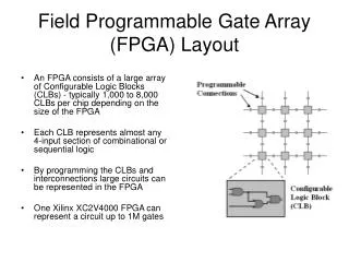
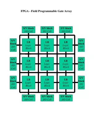
FPGA overview • 2-D array of logic blocks and flip-flops with programmable interconnections. • Compact design • User can configure • Intersections between the logic blocks • The function of each block
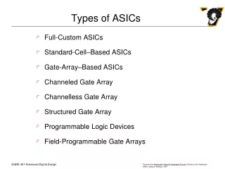
Why do we need FPGAs? • World of Integrated Circuits Full-Custom ASICs Semi-Custom ASICs User Programmable PLD FPGA
Which Way to Go? • ASICs FPGAs High performance Low development cost Low power Short time to market Low cost in high volumes Reprogrammable
Other FPGA Advantages • Manufacturing cycle for ASIC is very costly, lengthy and engages lots of manpower • Mistakes not detected at design time have large impact on development time and cost • FPGAs are perfect for rapid prototyping of digital circuits • Easy upgrades like in case of software • Unique applications
Programming Methodology • Electrically programmable switches are used to program FPGA • Properties of programmable switch determine on- resistance, parasitic capacitance, volatility, reprogram ability, size etc. • Various programming techniques are:- • SRAM programming technology • Floating Gate Programming • Anti fuse programming methodology
SRAM programming technologyUse Static RAM cells to control pass gates or multiplexers.1= closed switch connection 0= open For mux, SRAM determines the mux input selection process. Advantage • Fast re-programmability • Standard IC fabrication Tech. is used • Disadvantage • SRAM volatile • Requires large area
Why better ? • FPGA programmed using electrically programmable switches • Routing architectures are complex. • Logic is implemented using multiple levels of lower fan-in gates. • Shorter time to market • Ability to re-program in the field to fix bugs FPGA Disadvantage • FPGAs are generally slower than their application-specific integrated circuit (ASIC) • Can't handle as complex a design, and draw more power.
Application • Reconfigurable computing. • Applications of FPGAs include DSP, software-defined radio. • The inherent parallelism of the logic resources on the FPGA allows for considerable compute throughput.
FPGA Design and Programming • To define the behavior of the FPGA the user provides a hardware description language (HDL) or a schematic design. • Then, using an electronic design automation tool, a technology-mapped net list is generated. • The net list can then be fitted to the actual FPGA architecture using a process called place-and-route. • The user will validate the map, place and route results via timing analysis, simulation, and other verification methodologies. • Once the design and validation process is complete, the binary file generated used to configure the FPGA.