Download
1 / 12
150 likes | 275 Views
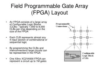
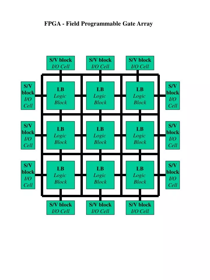
FPGA - Field Programmable Gate Array. S/V blo c k I/O Cell. S/V block I/O Cell. S/V block I/O Cell. S/V block I/O Cell. LB Logic Block. LB Logic Block. LB Logic Block. S/V block I/O Cell. S/V block I/O Cell. LB Logic Block. LB Logic Block. LB Logic Block.

E N D
FPGA - Field Programmable Gate Array S/V block I/O Cell S/V block I/O Cell S/V block I/O Cell S/V block I/O Cell LB Logic Block LB Logic Block LB Logic Block S/V block I/O Cell S/V block I/O Cell LB Logic Block LB Logic Block LB Logic Block S/V block I/O Cell S/V block I/O Cell LB Logic Block LB Logic Block LB Logic Block S/V block I/O Cell S/V block I/O Cell S/V block I/O Cell S/V block I/O Cell
Architecture of FPGA-s Symmetrical Array Row-based LB LB LB LB LB LB LB LB LB LB LB LB LB LB LB LB LB LB LB LB LB LB LB LB Hierarchical (CPLD) Sea-of-Gates PLA PLA PLA PLA PLA PLA PLA PLA
Example:realisation of the OR function based on LUT 0 1 1 X 1 1 X 2 Y 1 X 3 1 1 1 1 X 1 Y X 2 X 3
Logical block based on LUT-s LUT 0 T MUX 1 S LUT 0 T MUX 1 S
Example: realisation of function based on MUX-s. Y = X1 X2 + X1 X3 X1 X2 + X1 X3 X1 = 0 X1 = 1 X3 X2 X3 = 0 X2 = 1 X3 = 1 X2 = 0 0 1 1 0 MUX 0 0 1 1 X3 S MUX 0 Y X3 1 S MUX X2 1 0 X1 0 1 S X2
Interconnection resources Symmetrical FPGA LB LB CB Connection arrays CB SB CB CLK Connections between the neighbours LB LB CB Long lines
Row of interconnection resources in a FPGA with architecture Long lines over logical blocks LB LB LB LB LB LB For example, Actel-i Act-1, Act-2 FPGA-d
Interconnection resources in Sea-of-Gates type FPGA Neighbouring connections Connections in 4x4 blocks Cell Cell Cell Cell Cell Cell Cell Cell Cell Cell Cell Cell Cell Cell Cell Cell Cell Connections in the array Connections in 16x16 blocks 4x4 cell 16x16 I/O blocks I/O b l o c k s I/O b l o c k s I/O blocks For example. XILINX XC6200 and ACTEL-i ES serial arrays
Interconnection resources in CPLD type FPGA I/O blocks PLA PLA Local connection resources PLA PLA I/O blocks PLA PLA I/O blocks Local connection resource PLA PLA Global connection resource PLA Local connection resource PLA PLA PLA I/O blocks PLA PLA I/O blocks Logical block Local connection resource I/O blocks PLA PLA Macrocell
I/O cells 0 MUX T 1 S S/V contact I/O pad T 0 MUX 1 S
Designing of hardware based on FGPA . Description of the hardware. (Boolean functions Logical circuit, VHDL …) Logical optimization / minimisation Technology Mapping Placement Routing Programming / Configuring