Download
1 / 24
300 likes | 506 Views
Millimeter-wave load-pull techniques. ETH Zürich This work was supported in part by the Swiss National Science Foundation (SNSF) under Grant R’Equip 206021_144952/1 and Grant PMPDP2_139697 and by ETH Zürich under Scientific Equipment Program 03721. Outline. Introduction

E N D
Millimeter-wave load-pull techniques ETH Zürich This work was supported in part by the Swiss National Science Foundation (SNSF) under Grant R’Equip 206021_144952/1 and Grant PMPDP2_139697 and by ETH Zürich under Scientific Equipment Program 03721
Outline • Introduction • Basics of large signal characterization • Applications • Large Signal Characterization at high frequency • Existing solution examples • Pros and cons • A W-band on-wafer load-pull system • Block scheme • Calibration and accuracy verification • Measurement examples • Conclusions Introduction
Large signal Characterization Applications Basics • Many applications require measuring a few device performances in CW, while exciting its nonlinearities • Examples: • Performance/technology evaluation • Circuit design • Large signal models refinement • Reliability/failure tests • Production tests • Linear characterization (small signal) provides full information as long as the device under test (DUT) can be considered linear • e.g. passive components, transmission lines • Active devices show nonlinear behavior when excited in realistic (large signal) conditions • The extension of S-parameters to X-parameters might be too complicated • What information do we really need? Introduction
Basics of Large signal Characterization • We focus on the simplest example: a two port active device (a transistor in common source configuration) fed with a single CW tone @ f0 • Interesting performances: • DC power, PDC= VGSIG+VDSID • Output power: POUT=|b2|2 -|a2|2 @ f0, 2f0,…, nf0 • Gain = POUT/PIN@ f0 • Power added efficiency, PAE=(POUT- PIN)/PDC@ f0 • Influence parameters: • Bias point (DC supply) • Frequency f0 • Input power: PIN=|a1|2 -|b1|2 • GL =a2/b2@ f0, 2f0,…, nf0 Introduction
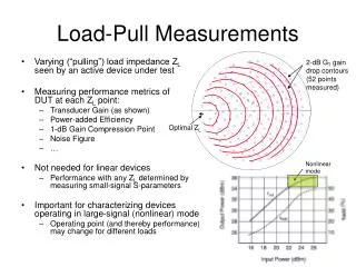
Load-pull measurements • A simplified block scheme of an on-wafer load-pull measurement system • On-wafer “environment” adds complications • calibration • additional losses Introduction
Load-pull calibration – vector calibration • Vector “VNA-like” calibration On-wafer or calibration substrate standards Introduction
Load-pull calibration – vector calibration • Vector “VNA-like” calibration On-wafer or calibration substrate standards Introduction
Load-pull calibration – power calibration • Power calibration WG or coax standards + power meter On-wafer or calibration substrate thru Introduction
Load-pull calibration • After calibration it is possible to modify the set up at the right of reflectometer 2 and at the left of reflectometer 1, without affecting calibration Introduction
Solutions for tunable loads ActiveLoad – open loop MechanicalTuners • Main issue: gamma limitation • Losses cannot be compensated • 2.5 dB losses reduce |G|=1 to |G|=0.56 • 0.2 dB losses reduce |G|=1 to |G|=0.95 • Main issue: gamma varies with POUT • Compensated by iterations Introduction
Solutions for tunable loads ActiveLoad – closedloop MechanicalTuners • Main issue: gamma limitation • Losses cannot be compensated • 2.5 dB losses reduce |G|=1 to |G|=0.56 • 0.2 dB losses reduce |G|=1 to |G|=0.95 • Main issue: possible oscillations • Reduced risk when losses are reduced Introduction
Load-pull measurements above 60 GHz References • E. Alekseev, D. Pavlidis, and C. Tsironis, “W-band on-wafer load-pull measurement system and its application to HEMT characterization,” in IEEE MTT-S, Baltimore, MD, USA, Jun. 1998, pp. 1479–1482. • D. W. Baker, et al., “On-wafer load pull characterization of W-band InP HEMT unit cells for CPW MMIC medium power amplifiers,” in IEEE MTT-S, Anaheim, CA, USA, Jun. 1999, pp. 1743–1746. • L. Boglione and R. T. Webster, “200 GHz fTSiGe HBT load pull characterization at mmwave frequencies,” in IEEE RFIC Symposium, Anaheim, CA, USA, Jun. 2010, pp. 215–218. • C. Li et al. “Investigation of loading effect on power performance for planar Gunn diodes using load-pull measurement technique,” IEEE MWCL, vol. 21, no. 10, pp. 556–558, Oct. 2011. • A. Pottrain, et al., “High power density performances of SiGe HBT from BiCMOS technology at W-band,” IEEE Electron Device Letters, vol. 33, no. 2, pp. 182–184, Feb. 2012. MechanicalTuners • Mechanical tuners exist (sold by main vendors) in the millimeter-wave range, up to 110 GHz • require pre-calibration • Including probe and set-up losses, 0.5-0.6 gamma is reachable on-wafer Large signal characterization
Load-pull measurements above 60 GHz • Open loop active loads combined with • 6-port measurements • Mixed signal measurement technique References ActiveLoads • S. A. Chahine, B. Huyart, E. Bergeault, and L. P. Jallet, “An active millimeter load-pull measurement system using two six-port reflectometers operating in the W-frequency band,” IEEE Trans. Instrum. Meas., vol. IM-51, pp. 408–412, Jun. 2002. • L. Galatro, M. Marchetti, M. Spirito, "60 GHz mixed signal active load-pull system for millimeter wave devices characterization," Microwave Measurement Symposium (ARFTG), 2012 80th ARFTG , vol., no., pp.1,6, 29-30 Nov. 2012. Large signal characterization
Load-pull measurements above 60 GHz • “In-situ” (integrated) • Still gamma limited • Integration required • no real-time References In Situ Tuners • T. V. Heikkil, J. Varis, J. Tuovinen, and G. M. Rebeiz, “W-band RF MEMS double and triple-stub impedance tuners,” in IEEE MTT-S Intl. Microwave Symp. Dig., Long Beach, CA, USA, Jun. 2005, pp. 923–926. • Y. Tagro, N. Waldhoff, D. Gloria, S. Boret, G. Dambrine, "In Situ Silicon-Integrated Tuner for Automated On-Wafer MMW Noise Parameters Extraction Using Multi-Impedance Method for Transistor Characterization," IEEE Transactions on Semiconductor Manufacturing, vol.25, no.2, pp.170,177, May 2012 • T. Quemerais, D. Gloria, S. Jan, N. Derrier, P. Chevalier, "Millimeter-wave characterization of Si/SiGe HBTs noise parameters featuring fT/fMAX of 310/400 GHz," Radio Frequency Integrated Circuits Symposium (RFIC), 2012 IEEE , vol., no., pp.351,354, 17-19 June 2012 Large signal characterization
94 GHz on-wafer active-loop load-pull system • Mechanical tuners with pre-calibration: less accurate than real-time • Mechanical tuners with real-time measurements: reduced gamma (0.5 maximum is typical) • In situ tuners: integration with the device / highly developed fabrication capabilities • Active loads with real-time measurements are a good solution, not yet widely diffused A W-band on-wafer load-pull system
94 GHz on-wafer active-loop load-pull system Realized at MWE laboratory, D-ITET, ETH Zürich, Switzerland A W-band on-wafer load-pull system
94 GHz on-wafer active-loop load-pull system • Simplified block diagram (*) • Novelty – the down-conversion-based active loop • Similar techniques exist to realize IF loads, at a few hundreds of MHz 94 GHz active-loop-based variable load (*) V. Teppati, H.-R. Benedikter, et al., “A W-Band On-Wafer Active Load-Pull System based on Down-Conversion Techniques”, IEEE Transactions on Microwave Theory and Techniques, Vo. 64, is.1, Jan. 2014, pp. 148-153. A W-band on-wafer load-pull system
Load-pull system calibration – step 1 • SW1 and SW2 in position 1 • On-wafer (or calibration substrate) standards are connected and measured A W-band on-wafer load-pull system
Load-pull system calibration – step 2 • SW1 in position 2 and SW2 in position 1, thru connection A W-band on-wafer load-pull system
Measurement Phase • SW1 in position 1 and SW2 in position 2 • It is possible to modify the set up (add a circulator, or a spectrum analyzer) at the right of reflectometer 2 and at the left of reflectometer 1, without affecting calibration A W-band on-wafer load-pull system
Residualerrorcomparison • A “thru” (on-wafer direct connection) should have 0 dB gain • Its gain variation vs. GL is taken as an estimation of the accuracy of the measurement A W-band on-wafer load-pull system
Measurement examples • 0.1x100µm2GaN HEMT • VDS=5 V, VGS=-3V (class A) Measurement examples
Measurement examples • 0.3x8.4µm2InP/GaAsSb DHBT • VCE=1.6 V, VBE=0.75 V (class AB) Measurement examples
Conclusions • Basics of large signal characterization • Mechanical tuners vs. active loads • Existing solutions for large signal characterization at high frequencies • W-band, down-conversion active loop, on-wafer load-pull system • accuracy • measurement examples