Download
1 / 72
720 likes | 991 Views
The single cycle CPU. Performance of Single-Cycle Machines. Memory Unit 2 ns ALU and Adders 2 ns Register file (Read or Write) 1 ns Class Fetch Decode ALU Memory Write Back Total R-format 2 1 2 0 1 6

E N D
Performance of Single-Cycle Machines • Memory Unit 2 ns • ALU and Adders 2 ns • Register file (Read or Write) 1 ns Class Fetch Decode ALU Memory Write Back Total R-format 2 1 2 0 1 6 LW 2 1 2 2 1 8 SW 2 1 2 2 7ns Branch 2 1 2 5ns Jump 2 2ns
What if we had a variable CK cycle? Let’s check the following scenario: • Rtype: 44%, LW: 24%, SW: 12% • BRANCH: 18%, JUMP: 2% • I- number of instructions in program • T- time of the CK cycle • CPI - number of CK cycle per instruction (=1) Execution=I*T*CPI= 8*24%+7*12%+6*44%+5*18%+2*2%=6.3 ns
The result: EXE Single cycle T single clock * I T single clock 8 EXE Variable T variable clock * I T variable clock 6.3 We get a ratio of 1.27. The ratio is higher when more complicated instructions, e.g., floating point instructions are also implemented. Since building a variable CK circuit is too complicated, we instead want instructions to take as many shorter CKs as required
Multicycle Approach • The idea of Multi-cycle approach: • We’ll save time since each instruction takes only the necessary number of CK cycles (which are about 5 times shorter than the original CK cycle) • We also save in components since we can use the same component in different phases of the same instruction
Building a Multi-Cycle CPU: Split the instruction to steps (phases) Make sure that the steps are balanced (same time required) Reduce the job done at each step. In each step only one chore is done. At the end of each CK cycle: Store the result of the current step to be used by the next step. So, add more internal registers for storing the intermediate results.
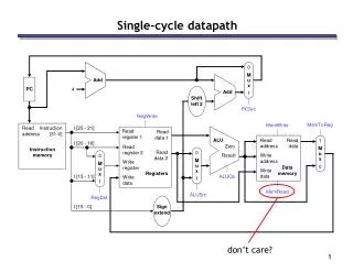
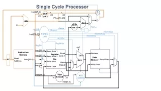
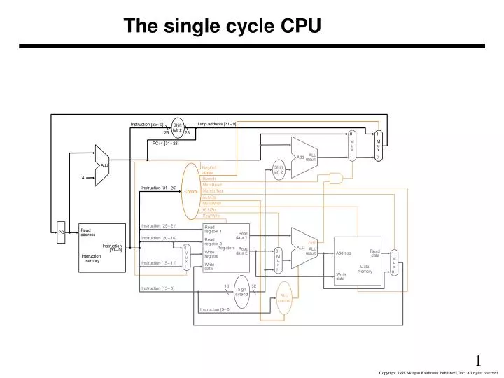
[25:21]=Rs [20:16]=Rt [25:21]=Rs 5 5 5 ck ck A single cycle CPU capable of R-type & lw/sw instructions (data & control) 4 MemWrite Adder [31:26] 6 add RegWrite [5:0]=funct 6 ALU control Reg File Data Memory Instruction Memory PC ALU Address D. Out 5 Rd D.In [15:0] 16 Sext 16->32
[25:21]=Rs [20:16]=Rt [25:21]=Rs 5 5 5 ck ck A single cycle CPU capable of R-type & lw/sw instructions - Data Path only 4 Adder Reg File Data Memory Instruction Memory PC ALU Address D. Out 5 Rd D.In [15:0] 16 Sext 16->32 lw sw
PC 0x400000 0x400004 I.Mem data Memory output new Memory output Rs, Rt ALU inputs new ALU inputs D.Mem adrs ALU output (address) New ALU output (new address) D. Mem data Mem data Mem data Write back Write back fetch execute memory fetch execute memory decode decode Timing of a single cycle CPU
Timing of a lw instruction in a single cycle CPU PC 0x400000 I.Mem data Memory output Rs, Rt ALU inputs D.Mem adrs ALU output (address) D. Mem data Mem data We want to replace a long single CK cycle with 5 short ones: fetch execute memory decode Write back 2ns 1ns 2ns 2ns 1ns 0 1 2 3 4 5=(0) PC 0x400000 fetch Instruction in IR IR decode ALU calculates something A,B execute Timing of a lw instruction in a multi-cycle CPU ALUout Mem data memory MDR Write back
ck ck Therefore we should add registers to the single cycle CPU shown below: 4 Adder Reg File [25:21]=Rs 5 Data Memory Instruction Memory PC ALU [20:16]=Rt 5 Address D. Out 5 Rd D.In [15:0] 16 Sext 16->32
ck ck ck ck ck ck ck Adding registers to “split” the instruction to 5 stages: 4 Adder A Reg File ALUout MDR [25:21]=Rs 5 Data Memory Instruction Memory PC ALU IR [20:16]=Rt 5 Address D. Out 2 5 Rd D.In PCWrite B 4 3 0 1 5 [15:0] 16 Sext 16->32
Here is the book’s version of the multi-cycle CPU: Only PC and IR have write enable signals All other registers hold data for a single cycle
IR[20:16]=Rt IR[25:21]=Rs 5 5 ck ck ck ck ck ck Here is our version of A mult--cycle CPU capable of R-type & lw/sw & branch instructions Reg File A Instruction & data Memory PC ALUout IR ALU 5 Rd B 4 IR[15:0] 16 Sext 16->32 << 2 MDR <<2
Let us explain the multi-cycle CPU • First we’ll look at a CPU capable of performing only R-type instructions • Then, we’ll add the lw instruction • And the sw instruction • Then, the beq instruction • And finally, the j instruction
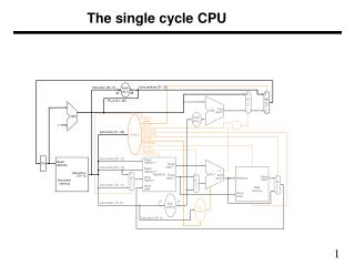
PC 0x400000 0x400004 Memory output New Memory output Rs, Rt ALU inputs new ALU inputs ALU output New ALU output Write back fetch execute decode [25:21]=Rs [20:16]=Rt [15:11]=Rd 5 5 5 ck ck Let us remind ourselves how works a single cycle CPU capable of performingR-type instructions.Here you see the data-path and the timing of an R-typeinstruction. 4 Adder [31:26] 6 Reg File Instruction Memory PC ALU [5:0]=funct 6
[25:21]=Rs [20:16]=Rt [15:11]=Rd 5 5 5 ck ck A single cycle CPU demo: R-type instruction 4 Instruction Memory Reg File ALU PC
ck ck ck ck ck A multi cycle CPU capable of performing R-type instructions Reg File A IR[25:21]=Rs 5 Instruction & data Memory PC ALUout IR ALU IR[20:16]=Rt 5 5 Rd B
ck ck ck ck ck A multi cycle CPU capable of R-type & instructionsfetch Reg File A IR[25:21]=Rs 5 Instruction & data Memory PC ALUout IR ALU IR[20:16]=Rt 5 5 Rd B 0 1
ck ck ck ck ck A multi cycle CPU capable of R-type & instructionsdecode Reg File A IR[25:21]=Rs 5 Instruction & data Memory PC ALUout IR ALU IR[20:16]=Rt 5 5 Rd B 1 2
ck ck ck ck ck A multi cycle CPU capable of R-type & instructionsexecute Reg File A IR[25:21]=Rs 5 Instruction & data Memory PC ALUout IR ALU IR[20:16]=Rt 5 5 Rd B 3 2
ck ck ck ck ck ck A multi cycle CPU capable of R-type & instructionswrite back Reg File A IR[25:21]=Rs 5 Instruction & data Memory PC ALUout IR ALU IR[20:16]=Rt 5 Rd 5 Rd B 3 4
PC 0x400000 Inst. Mem data Memory output = the instruction Timing of an R-type instruction in a single cycle CPU Rs, Rt ALU inputs ALU output (Data = result of cala.) GPR input fetch execute Write Back decode 0 1 2 3 4 (=0) PC Mem data Timing of an R-type instruction in a multi-cycle CPU fetch Previous inst. Current instruction IR decode A,B execute ALUout Write back
fetch PC Mem data Current instruction IR=M ( PC ) Previous inst. Current instruction next inst. IR decode GPR outputs A= Rs, B= Rt A,B execute ALU output ALUuot= A op B Write back Rd = ALUout ALUout At the rising edge of CK: Rd=ALUout R-Type instruction takes 4 CKs IRWrite The state diagram: A= Rs, B= Rt ALUout = A op B IR=M(PC) Rd=ALUout
IR[20:16]=Rt IR[25:21]=Rs 5 5 ck ck ck ck ck A multi-cycle CPU capable of R-type instructions (PC calc. ) Reg File A Instruction & data Memory PC ALUout IR ALU 5 Rd B 4
fetch current PC next PC = current PC+4 PC Mem data IR Previous inst. current instruction next inst. decode GPR outputs A,B execute ALU output Write back ALUout At the rising edge of CK: Rd=ALUout ALUuot = A op B PC = PC+4 PCWrite
ck ck ck ck ck A multi cycle CPU capable of R-type & instructionsfetch Reg File A IR[25:21]=Rs 5 Instruction Memory PC ALUout IR ALU ALU IR[20:16]=Rt 5 5 Rd B 4
The state diagram of a CPU capable of R-type instructions only Fetch 0 Decode 1 R-type ALU 6 WBR 7 IR=M(PC) PC = PC+4 A=Rs B=Rt ALUout=A op B Rd = ALUout
The state diagram of a CPU capable of R-type and lw instructions Fetch 0 Decode 1 lw R-type AdrCmp ALU 2 WB 6 lw Load 3 WBR 4 7 ALUout= A+sext(imm) MDR = M(ALUout) Rt = MDR
ck ck ck ck ck ck ck We added registers to “split” the instruction to 5 stages.Let’s discuss the lw instruction All parts related to lw only are blue 4 Adder A Reg File ALUout MDR [25:21]=Rs 5 Data Memory Instruction Memory PC ALU IR [20:16]=Rt 5 Address D. Out 2 5 Rd D.In PCWrite B 4 3 0 1 5 [15:0] 16 Sext 16->32 In ths single-cycle we kept the “data flow” from left to right. Here we change that a little, since as we’ll see, we are some parts of the CPU more than once during the same instruction. So we prefer to move data the memory.
IR[20:16]=Rt IR[25:21]=Rs 5 5 ck ck ck ck ck ck First we draw a multi-cycle CPU capable of R-type & lw instructions: Reg File A Instruction Memory PC ALUout IR ALU ALU ALU 5 Rd B 4 IR[15:0] 16 Sext 16->32 Data Memory MDR We just moved the data memory All parts related to lw only are blue
IR[25:21]=Rs IR[20:16]=Rt 5 5 ck ck ck ck ck ck A multi-cycle CPU capable of R-type & lw instructionsfetch Reg File A Instruction Memory PC ALUout IR ALU ALU ALU 5 Rd B 4 IR[15:0] Sext 16->32 16 Data Memory MDR
ck ck ck ck ck ck A multi-cycle CPU capable of R-type & lw instructionsdecode Reg File A IR[25:21]=Rs 5 Instruction Memory PC ALUout IR ALU IR[20:16]=Rt 5 5 Rd B 4 IR[15:0] 16 Sext 16->32 << 2 Data Memory MDR
IR[20:16]=Rt IR[25:21]=Rs 5 5 ck ck ck ck ck ck A multi-cycle CPU capable of R-type & lw instructionsAdrCmp Reg File A Instruction Memory PC ALUout IR ALU ALU 5 Rd B 4 IR[15:0] 16 Sext 16->32 Data Memory MDR
IR[25:21]=Rs IR[20:16]=Rt 5 5 ck ck ck ck ck ck A multi-cycle CPU capable of R-type & lw instructionsmemory Branch Address Reg File A InstructionMemory PC ALUout IR ALU 5 Rd B 4 IR[15:0] 16 Sext 16->32 << 2 Data Memory MDR
IR[25:21]=Rs IR[20:16]=Rt 5 5 ck ck ck ck ck ck ck A multi-cycle CPU capable of R-type & lw instructionsWB Reg File A InstructionMemory PC ALUout IR ALU Rt 5 Rd B 4 IR[15:0] 16 Sext 16->32 Data Memory MDR
IR[20:16]=Rt IR[25:21]=Rs 5 5 ck ck ck ck ck ck ck Can we unite the Instruction & Data memories? (They are not used simultaneously as in the single cycle CPU) Reg File A InstructionMemory PC ALUout IR ALU 5 Rd B 4 IR[15:0] 16 Sext 16->32 Data Memory MDR
IR[20:16]=Rt IR[25:21]=Rs 5 5 ck ck ck ck ck ck So here is a multi-cycle CPU capable of R-type & lw instructionsusing a single memory for instructions & data Reg File A Instruction & data Memory PC ALUout IR ALU 5 Rd B 4 IR[15:0] 16 Sext 16->32 MDR
PC 0x400000 I.Mem data Memory output Timing of a lw instruction in a single cycle CPU Rs, Rt ALU inputs D.Mem adrs ALU output (address) D. Mem data Mem data fetch execute memory decode Write back PC PC+4 fetch current instruction IR Previous inst. Timing of a lw instruction in a multi-cycle CPU decode A,B execute Data address ALUout Mem data memory Data to Rt MDR Write back
fetch PC IR=M ( PC ) PC= PC+4 Mem data IR Previous inst. current instruction decode GPR outputs A= Rs, B= Rt A,B execute ALU output Data address ALUuot= A+sext(imm) ALUout Data address memory Mem data MDR=M(ALUout) Write back Data to Rt MDR At the rising edge of CK: Rt=MDR PCWrite, IRWrite
The state diagram of a CPU capable of R-type and lw instructions WB IR=M(PC) PC = PC+4 Fetch 0 A=Rs B=Rt Decode 1 lw R-type ALUout= A+sext(imm) AdrCmp ALU ALUout=A op B 2 6 Load MDR = M(ALUout) 3 WBR Rt = MDR Rd = ALUout 4 7
IR[25:21]=Rs IR[20:16]=Rt 5 5 ck ck ck ck ck ck A multi-cycle CPU capable of R-type & lw & sw instructions Branch Address Reg File A Instruction & data Memory PC ALUout IR ALU 5 Rd B 4 IR[15:0] 16 Sext 16->32 << 2 MDR lw sw
The state diagram of a CPU capable of R-type and lw and sw instructions Fetch 0 Decode 1 lw+sw R-type AdrCmp ALU 2 WB 6 lw sw Load Store 3 5 WBR 4 7 IR=M(PC) PC = PC+4 A=Rs B=Rt ALUout= A+sext(imm) ALUout=A op B M(ALUout)=B MDR = M(ALUout) Rd = ALUout Rt = MDR
IR[20:16]=Rt IR[25:21]=Rs 5 5 ck ck ck ck ck ck A multi-cycle CPU capable of R-type & lw/sw & branch instructions Reg File A Instruction & data Memory PC ALUout IR ALU 5 Rd B 4 IR[15:0] 16 Sext 16->32 <<2 IR
Adding the instruction beq to the state diagram: Fetch 0 Decode 1 lw+sw beq R-type AdrCmp Branch ALU 2 8 WB 6 lw sw zero Load not zero Store 3 5 WBR 4 7 Calc Rs -Rt (just to produce the zero signal) Calc PC=PC+sext(imm)<<2
Fetch 0 Calc ALUout=PC+sext(imm)<<2 Decode 1 lw+sw beq R-type AdrCmp Branch ALU 2 8 WB 6 lw sw Load Store 3 5 WBR 4 7 Adding the instruction beq to the state diagram, a more efficient way: Let’s use the decode state in which the ALU is doing nothing to compute the branch address.We’ll have to store it for 1 more CK cycle, until we know whether to branch or not! (We store it in the ALUout reg.) Calc Rs - Rt. If zero, load the PC with ALUout data, else do not load the PC
IR[25:21]=Rs IR[20:16]=Rt 5 5 ck ck ck ck ck ck A multi-cycle CPU capable of R-type & lw/sw & branch instructions PC+4 Reg File A Instruction & data Memory PC ALUout IR ALU 5 Rd B 4 IR[15:0] 16 Sext 16->32 <<2 IR Branch Address
Adding the instruction j to the state diagram: WB Fetch 0 Decode 1 j lw+sw beq R-type Jump AdrCmp Branch ALU 9 2 8 6 lw sw Load Store 3 5 WBR 4 7 PC = PC[31:28] || IR[25:0]<<2
IR[20:16]=Rt IR[25:21]=Rs 5 5 ck ck ck ck ck ck A multi-cycle CPU capable of R-type & lw/sw & branch & jump instructions PC+4= next address IR[25:0] Jump address <<2+ PC[31:28] Reg File A Instruction & data Memory PC ALUout IR ALU 5 Rd B 4 IR[15:0] 16 Sext 16->32 <<2 IR Branch Address
The phases (steps) of all instructions 0 1 6 2 8 9 3 7 4 5