Download
1 / 23
260 likes | 601 Views
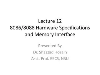
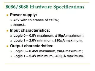
8088 Microprocessor Hardware. Address Bus. Data Bus. Control Bus. Microprocessor System Modules. Keyboard Monitor Printer Mouse Microphone Disk LED LCD SWICH. CPU. Memory (RAM, ROM). Peripherals (IO). Von Neumann Architecture. Microprocessor. Memory. Address Lines.

E N D
Address Bus Data Bus Control Bus Microprocessor System Modules Keyboard Monitor Printer Mouse Microphone Disk LED LCD SWICH CPU Memory (RAM, ROM) Peripherals (IO)
Von Neumann Architecture Microprocessor Memory Address Lines Data Lines Control Lines
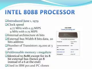
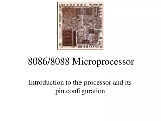
The 8088 Features • Has 20 address lines so could address up to 1 Mb of memory ( ) at a time when 8085 could only address 64 kb. • The 8088 CPU was the first chip used in IBM’s microcomputers
Power and Ground Pins • Vcc – pin 40 • Gnd – pin 1 and 20
Address Pins • AD0..AD7 • A8..A15 • A19/S6, A18/S5, A17/S4, A16/S3
Data Pins • AD0..AD7
Control Pins • MN/MX’ (input) • Indicates what mode the processor is to operate in • READY (input) • When given an input LOW, it will go into a wait state • CLK (input) • Provides basic timing for the processor • needed by the microprocessor to synchronize signals • ideally a square wave having a constant frequency • RESET (input) • Causes the processor to immediately terminate its present activity • To reset the microprocessor, this must be HIGH for at least 4 clock cycles
Control Pins (Continue) • HOLD (input) • Connect this to LOW • HLDA (Hold Acknowledge) Active-high output signal. After input on HOLD, the CPU responds with HLDA to signal that the DMA controller can use the buses.
Control Pins (Continue) • INTR (input) • Interrupt request • INTA’ (output) • Interrupt Acknowledge • NMI (input) • Non-maskable interrupt
Control Pins (Continue) • DEN’ (output) • Data Enable • It is LOW when processor wants to receive data or processor is giving out data • DT/R’ (output) • Data Transmit/Receive • When HIGH, direction of data lines is from microprocessor to memory/devices • When LOW, direction of data lines is from memory/devices to microprocessor • IO/M’ (output) • Device/Memory • When HIGH, microprocessor wants to access I/O Device • When LOW, microprocessor wants to access memory
Control Pins (Continue) • RD’ (output) • When LOW, it indicates that the microprocessor is performing a read access • WR’ (output) • When LOW, it indicates that the microprocessor is performing a write access • ALE (output) • Address Latch Enable • Provided by the microprocessor to latch address • When this is HIGH, microprocessor is using AD0..AD7, A19/S6, A18/S5, A17/S4, A16/S3 as address lines
At what address does the 8088 wake up Physical Address=CS*16+IP=FFFF*16+0000=FFFF0+0000=FFFF0
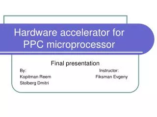
طراحی گذرگاه کنترل در مد مینیمم 8088 ------- IORD --------- IOWR ----------- MEMRD ----------- MEMWR
نحوه جداسازی باس آدرس از باس داده بدلیل محدودیت در تعداد پینها، باس های داده و آدرس مالتی پلکس شده اند. برای جداسازی باسها از یک لچ 8 بیتی و سیگنال ALE استفاده میکنیم. سیگنال ALE(Address Latch Enable): سیگنال خروجی Active – High نشان میدهد یک آدرس معتبر بر روی باس آدرس قرار داده شده است.
Processor Timing Diagram of 8088 (Minimum Mode)for Memory Read T1 T2 T3 T4 CLOCK __ DT/R ALE AD7 - AD0 A7 - A0 D7 - D0 (from memory) A15 - A8 A15 - A8 A19/S6 - A16/S3 A19 - A16 S6 - S3 __ IO/M ____ RD ______ DEN
D7 - D0 Q7 - Q0 GND OE 74LS373 LE D7 - D4 Q7 - Q4 D3 - D0 Q3 - Q0 GND OE 74LS373 LE نحوه جداسازی باس آدرس از باس داده Minimum Mode D7 - D0 DEN DT / R AD7 - AD0 A7 - A0 A15 - A8 A19 - A16 A15 - A8 MEMORY 8088 A19/S6 - A16/S3 ALE RD RD IO / M WR WR
بافر کردن باس داده برای این منظور از بافر دو جهته (Transciever)74245 استفاده میکنیم. Transciever: Transmitter/Reciever
Home Work فصل ریزپردازنده های 8088/86 و تراشه های پشتیبان از کتاب مزیدی مسائل: 14-15-17-38-40-42-46 مهلت تحویل: 3 هفته