Download
1 / 12
120 likes | 208 Views
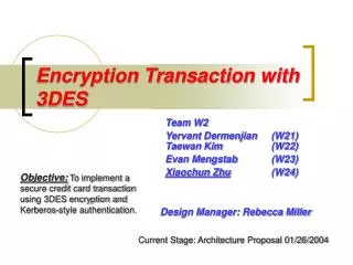
Encryption Transaction with 3DES. Team W2 Yervant Dermenjian (W21) Taewan Kim (W22) Evan Mengstab (W23) Xiaochun Zhu (W24). Objective: To implement a secure credit card transaction using 3DES encryption using Kerberos-style authentication. Design Manager: Rebecca Miller.

E N D
Encryption Transaction with 3DES Team W2 Yervant Dermenjian (W21)Taewan Kim (W22) Evan Mengstab (W23) Xiaochun Zhu (W24) Objective: To implement a secure credit card transaction using 3DES encryption using Kerberos-style authentication. Design Manager: Rebecca Miller Current Stage: Full Chip SPICE Simulation03/31/2004
Current Status • Design Proposal (100% done) • Architecture Proposal (100% done) • Size Estimate and Floor Plan (100% done) • Full-chip Transistor-level Schematic (100% done) • Component Layout & Simulation (100% done) • Top-Level Layout (100% done) • Spice simulation of the entire chip (Successful) • Need to find maximum frequency
Simulation Strategy • Simulate Entire Chip • Use same inputs from C and Verilog verification • Encryption ensures multiple vectors over critical path • Each iteration tests different pattern over critical path • Each time an iteration is run, SBOX determines new values that will initiate critical path • Run simulation for 20 clock cycles • Will not produce final output but… • Values at each node should match Verilog
Critical Path Mux -> Expand -> XOR -> SBOX -> XOR -> Mux 00000000D8D8DBBC D8D8DBBCE73AED4F 80FF828E80FFC887 80FB848480FFC68C 80FFC68C0905717
Spice Simulation 100 MHz simulation
Close Ups 214ps 340ps
Problems Simulating • No DC path to ground errors • Loose wires • Quota exceeded errors • Clear /tmp • Increase quota • Simulation file inputs do not increase piecewise linearly • Error in Java sim file generator • Degredation of Vdd! away from pin • Modules near vdd! pin work correctly • Modules further away have a lower vdd! Do not pass full 1.8 volts when PMOS passes vdd signal
Vdd! Problems Actual lengths from top level design • Simulation of Program Control and ROM using vdd! and gnd! wiring from top-level • Outputs all very low 400mV
Vdd! Problems Doubling the wiring should halve the resistance • Simulation of Program Control and ROM using twice the wiring • Output correct with maximum value of 1.5 volts 1.5 volts
Vdd! Problems Extremely low resistance 1.8 volts • Simulation of Program Control and ROM using very wide vdd! and ground wires • Output correct with maximum value of 1.8 volts
Conclusions / Solutions • Conclusions • Vdd and Ground are not assumed to be infinite strength • Vdd strength decreases as distance from pin increases • Solutions • Increase thickness of Vdd and Ground rails • Add more Vdd and Ground connections • Status • Changes were made • Simulation successful at 100MHz • Need to test higher clock speeds to find maximum