Download

1 / 18
210 likes | 487 Views
Encryption Transaction with 3DES. Team W2 Yervant Dermenjian (W21) Taewan Kim (W22) Evan Mengstab (W23) Xiaochun Zhu (W24). Objective: To implement a secure credit card transaction using 3DES encryption using Kerberos-style authentication. Design Manager: Rebecca Miller.

E N D
Encryption Transaction with 3DES Team W2 Yervant Dermenjian (W21)Taewan Kim (W22) Evan Mengstab (W23) Xiaochun Zhu (W24) Objective: To implement a secure credit card transaction using 3DES encryption using Kerberos-style authentication. Design Manager: Rebecca Miller Current Stage: Short Final Presentation04/12/2004
Status Update • Have not found source of voltage drop on Vdd problem • Debugging Attempts • 1) Simulate PC alone with long Vdd & Gnd rails: Works • 2) Simulate (1) with min sized buffers on input AND output: Works • 3) Simulate PCROM alone with long Vdd & Gnd rails: Works • 4) Simulate (3) with min sized buffers on input AND output: Works • 5) Simulate PC & PCROM together without resistances: Works • 6) Simulate PC & PCROM together with resistances: Doesn't Work • 7) Remove excess M1 to Gnd contacts in ROM and decoder in (6): Doesn't Work • 8) Do (7) with NWell and contacts along long Vdd rail: Works • They’re connected by a few microns of wire: Shouldn’t be a problem • Workaround: Layed Vdd and Gnd rails everywhere possible • Runs at 150MHz
Project Description • Implement Triple DES Encryption using 0.18μCMOS technology • Attain speeds appropriate for application in Automated Teller Machines (200MHz) • Integrate Encryption into ATM transation • Use Kerberos-style authentication • Encrypt User Information as data using CC# and Pin as Keys • Transaction Authorizer decrypts using CC# and Pin (which they know) • Credit Card Number and PIN are never transmitted, but are essential to authenticate
Marketability • Point-of-sale terminals transmit your name, credit card number, and expiration dates ‘in the clear.’ • Credit and charge card fraud costs cardholders and issuers hundreds of millions of dollars each year • Using Kerberos-style authentication, we transmit encrypted information that can be verified by the card authorizer without actually containing sensitive information. • Uses existing cards and phone network • Finalist for the 2001 Advanced Encryption Standard • April 1, 2005 – MasterCard requires all ATMs be 3DES compliant
System Integration Triple DES Compliant Unencrypted Card# + PIN Verified Verified Triple DES Encryption Encrypted Card# + PIN Encrypted Card# + PIN
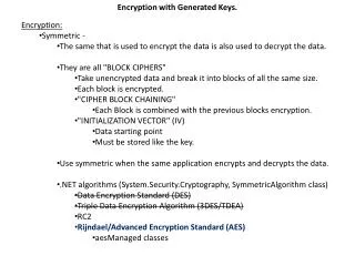
The 3DES Algorithm • Overview • Block Cipher - acts on a 64-bit block of plaintext • Converts it into a 64-bit block of cipher text using a 56-bit key • Specified in FIPS Pub 46-3 • Symmetric Key Cipher – encryption & decryption use same key • DES vs. 3DES • 3DES applies 3 stages of DES with a separate key for each stage • Total key length in 3DES is 56 bits x 3 key = 168 bits • Stages • Stage 1: Encrypt plaintext with Key 1 • Stage 2: Decrypt cipher text from Stage 1 with Key 2 (produces new cipher text) • Stage 2: Encrypt cipher text from Stage 2 with Key 3
DES DES-1 DES 3DES Algorithm Flowchart (I) Encryption Cipher Text K3 Plain Text K2 K1 DES-1 DES DES-1 Decryption
3DES Algorithm Flowchart (II) 64 bit plain Text Extension 32 bit 48 bit Left Half Initial Permutation Sub key 48 Bit XOR 16 Rounds Encryption S Box 32 Bit XOR Final Permutation Right Half Single Round cipher Text
3DES Algorithm Flowchart (III) Key Schedule 56bit Key Initial Permutation I=1 I=I+1 Left/Right Half 28 bits Left Barrel Shift N I=16? Final Permutation Y Ready 48 bit Sub-key [ I ]
Revised Floorplan Final Floorplan M1 M2 M3 M4 Original Floorplan 367μm Input Mux 56’b 2:1 mux 56’b Key Latch 64’b 2:1 demux 32’b Latch Mux Output Left Barrel Shifter 56’b Right Barrel Shifter 56’b Mux 32’b Text Register (L) 32’b Text Register (R) 48’b XOR IP IP-1 32’b Mux P 64’b 2:1 mux PC1 KeySub 56’b Register 56’b Key Reg PC2 32’b XOR Expand 56’b 2:1 mux PC (wiring) 64 -> 56 PC-2 wiring 56b -> 48b Input PC (wiring) 64 -> 56 Enc_ShiftL Dec_ShiftL 64’b 2:1 demux Output IP-1 Wiring Input 32’b 2:1 mux 56’b 2:1 mux Total Area: 111947 um2 = 0.112mm2 56’b 2:1 mux KeySub 56’b Register 56’b 2:1 mux 56’b Key Latch PC-2 wiring 56b -> 48b Density .09 Trans/um2 Output Enc_ShiftL Des_ShiftR 415 um All large functional blocks use Metal 1 and Metal 2. 377.44 um 32’b Latch 32’b Mux Expand IP (wiring) 32’b 2:1 mux S-box 512 x 4’b 64’b 2:1 mux 48’b XOR Data Reg (R) 32’b Data Reg (L) 32’b Transistor Density: 0.136 trans/ um2 P Wiring S-box 512 x 4’b Program Control (Instruction ROM) Program Control (Instruction ROM) 32’b 2:1 mux 32’b 2:1 demux 32’b XOR 48’b XOR IP (wiring) Expand 64’b 2:1 mux 32’b 2:1 demux Text 64’b Reg 125,534 um2 = .126 mm2 clock 379μm Program Control 334.37 um 32’b XOR P Wiring 269 um IP-1 Wiring
Expected Output : 2f 81 a8 bf 3c 6b df b4 Verification • Verify • C Simulation • Behavioral • Schematic • Layout C code Verification Structural Verification Behavioral Verification
Problems Encountered • Layout • Interconnections between components back and forth due to complicated algorithm • Permutations take too much space • Spice Simulation • Vdd Strength drops along conductor wires • No DC path to ground from node
Overall Chip Specifications • Input Pins • 32 Data Pins (used for input text and keys) • 1 Clock Pin • 1 Reset Pin (asserted high) • 1 Vdd Pin • 1 Ground Pin • Output Pins • 32 Cipher Text Pins (64’b cipher text delivered over 2 clocks) • 1 Valid Output Pin • 1 Get Next Key Pin • Total Pin Count: 70 • Chip Aspect Ratio: 1.03 • Chip Area: 139093 μm2 = 0.139093 mm2 • Total Transistor Count: 13,697 (PMOS: 4,324 NMOS: 9,373) • Transistor Density: 0.09847 transistors/μm2 = 10.155 μm2/transistor • Operation: 256’b Input 64’b Output over 54 clock cycles • Faster Clock Speed: 150MHz • Total Throughput: 169.54 Mbits / second
Full Chip Layout Text Register S BOX ROM and Decoders PC2 Perumtation Expand Permutation Initial Permutation P Permutation Barrel Shifting Final Permutation Initial Permutation Input Latch Key Register XOR Program Control
Final Presentation Breakdown • Marketing Evan • Algorithm Description Xiaochun • Design Process Evan • Floorplan Evolution Taewan • Verification Taewan • Issues Yervant • Specifications Xiaochun • Layout Yervant • Conclusions Yervant