Download
1 / 5
231 likes | 889 Views
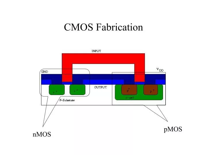
pMOS. nMOS. CMOS Fabrication. The fabrication process consists of a series of steps in which layers of the chip are defined through the photolithography process. Inverter can be described as having six masks namely: n-well Polysilicon n + diffusion p + diffusion Contacts and metal.

E N D
pMOS nMOS CMOS Fabrication
The fabrication process consists of a series of steps in which layers of the chip are defined through the photolithography process. Inverter can be described as having six masks namely: n-well Polysilicon n+ diffusion p+ diffusion Contacts and metal The first processing step is that of oxidation (allows for protection of regions that need not be doped). Form an n-well using a Group V element (this changes substrate from p-type to n-type to accommodate the pMOS). Region devoid of the SiO2 get doped. Dopants can be introduced into the wafer by diffusion or ion implantation. The Fabrication Process
Layout design rules describe device dimensions and how close different and like layers can be brought to close proximity without creating shorts. The lambda based design rules made popular by Mead and Conway are based on the single parameter l and permit for ease of scaling. Industry used micron as a unit of measure and this makes scaling difficult since not all dimensions do not scale uniformly. Lambda (l) is generally half of the minimum drawn transistor channel length. The channel length describes the distance between the inside edges of the source and drain. It is set by the minimum poly width. We are begin to refer to the gate channel length in nanometers (nm) whereas for technologies 0.18 mm and above we used the micron. Layout Design Rules
Lambda rules allow for ease of migrating designs from one technology node to another. Our Cad Tools in the Lab measure in micron. Academia relies on MOSIS (fabrication house (foundry)) to fabricate their designs. MOSIS provides a comprehensive summary of scalable CMOS (SCMOS) rules at http://www.mosis.org These rules cover a wide range of manufacturing processes. The rules define minimum wire widths to avoid breaks, minimum spacing to avoid shorts between neighboring wires and minimum overlap to minimize parasitic capacitance. Contacts have traditionally been kept at 2l X 2l for different technology generations. Polysilicon has a minimum width of 2l and must overlap diffusion by 2l and must be 1l away from the next poly wire. Layout Design Rules
To lesson the possibility of having layers of the same material creating short circuits, it is best to have same layers oriented in the same direction (metal1 placed horizontally while poly runs vertically). Gate Layout VDD GND