Download

1 / 31
480 likes | 932 Views
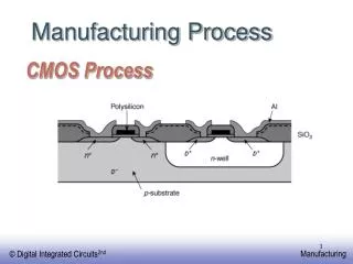
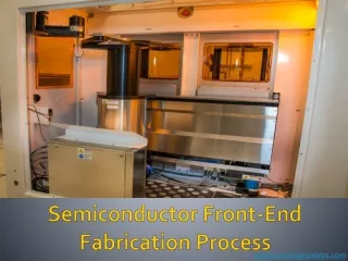
Twin Well CMOS Fabrication Process. In this lecture, you will learn the process integration in the fabrication of CMOS transistors. Read : C.Y. Chang and S.M. Sze “ULSI Technology”,McGraw-Hill, (1996), pp. 473-495.

E N D
In this lecture, you will learn the process integration in the fabrication of CMOS transistors • Read : • C.Y. Chang and S.M. Sze “ULSI Technology”,McGraw-Hill, (1996), pp. 473-495. • R.C. Jaeger, “Introduction to Microelectronic Fabrication” Prentice-Hall (2002), pp. 7-10.
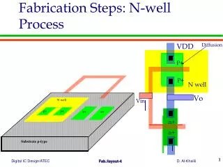
1. Formation of N-well • The starting material is a lightly doped p-type silicon wafer. A thin stress release oxide (SRO) is grown, followed by the deposition of a silicon nitride layer by low pressure chemical vapour deposition (LPCVD). A window is defined in the nitride by photolithography and etched by reactive ion etching (RIE). • A phosphorus implantation is carried out, with the nitride layer acting as a mask. The phosphorus ions are implanted into the exposed region, which will eventually form the n-well.
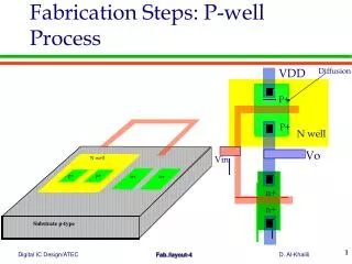
2. Formation of P-well • A wet oxidation is performed. A thick oxide is grown on the part of the wafer not covered by the nitride, while the oxide on the covered part remains thin. This is the local oxidation of silicon (LOCOS) process. • The nitride layer is removed by wet etching. A boron implantation is then carried out, with the thick oxide (covering the n-well) acting as a mask. The boron ions are implanted into the exposed region, and driven in by diffusion to form the p-well. • Note that only one mask is used and the two wells are self-aligned.
3. Channel Stop Implant • The oxide is stripped off and a new stress release oxide grown, followed by LPCVD of a silicon nitride layer. The nitride layer is patterned by photolithography the part outside the active device area is etched off. • A second photolithography step is used to cover the n-well. A high dose boron implantation is performed to convert the part of the p-well adjacent to the n-well into a heavily doped p+ region.
4. Field Oxide Growth A thick field oxide is grown by LOCOS in the region exposed by the nitride layer. The purpose of this field oxide and the channel stop implant is to prevent the formation of a parasitic MOSFET between the active regions of the CMOS devices.
5. Gate Poly Definition The stress release oxide is stripped off. A thin, good quality oxide is grown as the dielectric of the CMOS devices. A polysilicon layer is deposited by LPCVD and doped heavily with phosphorus. A photolithographic step is performed to define the polysilicon gates, with the rest of the polysilicon etched away by RIE. The gate polysilicon is partially oxidised.
N-Lightly Doped Drain (LDD) Implant • A photolithography step is used to cover the p-MOS part of the structure. A low dose phosphorus implantation is performed to form the lightly-doped drain-source extension regions of the nMOS, which are self-aligned to the gate.
7. P-Lightly Doped Drain (LDD) Implant A photolithography step is used to cover the n-MOS part of the structure. A low dose boron implantation is performed to form the self-aligned, lightly-doped drain-source extension regions of the pMOS.
8. Spacer Formation • An undoped oxide layer is deposited by LPCVD using tetraethyl orthosilane (TEOS). TEOS depositions have very good step coverage and uniformity. The chemical reaction of the process is as follows : • Si(C2H5O)4 + 12O2 SiO2 + 8CO2 + 10H2O • An anisotropic etch of the oxide by RIE is carried out to remove all the oxide, except those on the sidewalls of the polysilicon gates. These will act as spacers for the drain-source implantation masks.
9. Source Drain Implant of nMOS Device • A thin sacrificial oxide is grown . The pMOS structure is covered by photoresist following photolithography. A high dose arsenic implantation is carried out, using the polysilicon gate and the side walls as the mask, to form the highly doped source-drain regions of the nMOS device.
10. Source Drain Implant of pMOS Device A similar process is carried out with the next masking step and boron implantation to form the highly doped source-drain regions of the pMOS device. After this, the sacrificial oxide layer is etched.
11. Salicide Process • A thin titanium is deposited on the surface by physical vapour deposition (PVD). The wafer is then subjected to rapid thermal processing (RTP), during which it is heated up to a temperature between 600C and 800C. At this temperature, those titanium that is in contact with silicon and polysilicon will react to form titanium silicide, while those that is in contact with SiO2 will not react. The unreacted titanium is then removed by an etchant that attacks titanium by not titanium silicide. • Titanium silicide has a low resistivity and is used to reduce the resistance of the gate, as well as the contact resistance of the drain / source regions. In this process, the titanium silicides are self-aligned to the gate, drain and source regions, hence this is a self-aligned silicidation process.
12. Passivation and Contact Etch • The wafer surface is covered by a borophosphosilicate glass (BPSG) deposited by LPCVD. This is to passivate the surface, especially against alkali ions and it is effective in immobilising these ions. It also improves step coverage. • Windows are etched through the BPSG for making contacts to the drain and source regions of the CMOS devices.
13. First Layer Metallisation • Metal contacts are deposited by PVD and defined by photolithography to contact the drain and source regions of the CMOS devices.
14. Passivation and Planarisation The first layer metal is covered by a dielectric, and is planarised by chemical-mechanical polishing (CMP). Via holes are etched in the dielectric and metal lines deposited and defined. The metal is in turn covered by another passivation layer. Multiple layers of metals and dielectrics are deposited and defined for interconnections of the devices on an IC chip.
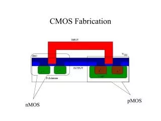
Link to the Flash animation on twin well CMOS fabrication: CMOS Fabrication