Download
1 / 31
310 likes | 498 Views
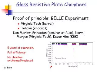
Development of a DHCAL with Resistive Plate Chambers. Jos é Repond Argonne National Laboratory. American Linear Collider Workshop Cornell University, Ithaca, NY July 13 - 16, 2003. I. Introduction. Collaboration. Argonne National Laboratory

E N D
Development of a DHCAL with Resistive Plate Chambers José Repond Argonne National Laboratory American Linear Collider Workshop Cornell University, Ithaca, NY July 13 - 16, 2003
I. Introduction Collaboration Argonne National Laboratory I Ambats, G Drake, V Guarino, J Repond, D Underwood, B Wicklund, L Xia Fermilab C Nelson, R Yarema, (A Para, V Makeeva) Boston University J Butler, M Narain University of Chicago K Anderson, E Blucher, J Pilcher, M Oreglia, H Sanders, F Tang
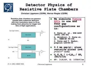
Design considerations Multi-gap smaller signals less streamers improved longevity reduced cross-talk better rate capability Avalanche mode smaller signals improved longevity reduced cross-talk no multiple-streamers better rate capability High-resistive graphite layer reduced cross-talk
Test chamber design and construction Gas mixture Freon/Argon/IsoButane = 62:30:8
Cosmic Ray test set-up Trigger Cosmic ray telescope with 4 layers of scintillator Rate ~1Hz Data acquisition Charge integration Gate between 700 ns and 20μs Readout up to ~40 channels Alternative tests Amplifier, shaper, discriminator
II. Tests with single pads Avalanche mode Total charge of signal increases with HV At 7.4 kV Signal ~ 0.2 pC
…and streamer mode Total charge of signal increases with HV At 8.0 kV Signal ~ 10 pC Significant amount of multi-streamers and of avalanches
Measurements of efficiencies Charge integration Discriminator Efficiency greater than 90% in avalanche mode (plateau ~300V) Small fraction of streamers Noise rate ~50Hz for avalanche mode Efficiency greater than 90% in avalanche mode (plateau ~200V) Small fraction of streamers
Central pad 1 x 1 cm2 All 1 x 5 cm2 Pads added together Big pad 19 x 19 cm2 III. Analysis of Multi-pad Data Readout system and analysis RABBIT system Records charges Calibration: 1.1fC/ADC count Pedestal subtracted Negative values set to zero Pad structure Data sets AIR2 38 kEvents 2 gaps of 0.64 mm glass of 1.1 mm R□ ~ 1.2 MΩ AIR1 24 kEvents same as above R□ ~ 200kΩ Default
Summing up all charges Assume pad with highest charge ≡ pad hit Clear avalanches and streamers Significant charge outside pad hit
Neighbors… Pad hit sees more charge than any neighbor Much worse for AIR1 with low R□ Only central 9 pads Charge in neighbor correlated with charge of pad hit
Central pad 1 x 1 cm2 All 1 x 5 cm2 pads added together Big pad 19 x 19 cm2 Central pad with maximum charge Zeros: cut out Avalanches Streamers: just a few
Central pad with maximum charge: select avalanches All pads at a given distance from central pad added up Similar results for streamers Error bars are RMS of distributions Charges go negative
Central pad with maximum charge: select avalanches Looking at individual pads Average charge on neighboring pads small
Central pad with maximum charge: select avalanches Counting pads with charge > Q0 Mostly direct neighbors No counts in second ring <Multiplicity> High Increases with charge in central pad 2 x 2 cm2 will work (charge small outside R = 1 cm) Measurements need to be repeated with discriminators
IV. Amplifier Tests on RPCs Goals • See real signal shapes • Compare signals on adjacent and far pads • Determine shape of “cross talk” signals • Compare performance of fast and slow amplifiers
Set-up 2 pairs of adjacent pads with fast amplifiers slow analog amplifiers on pads between and around Amplifiers • MAX3760 600 MHz, 6 kΩ gain (fast) •AD8015 250 MHz, 10 kΩ gain (slower) • UPC1663 Video amplifier with 30 ns integration time (cheap) • CDF Rabbit ADCs with 700 to 2000 ns integration Readout •Measure rates with discriminators/latches •Record signals on fast digital oscilloscope
Typical connection for measuring rates • All instrumented pads can be latched at each cosmic trigger Note: MAX3760 has very good timing, but saturates
A few traces from cosmic rays 10 ns/division Raw signal in AD8015 Signal in slow video amplifier Note induced signal of opposite sign in far away pad
Some results • In 30% of the events, same sign signal observed in adjacent pad (depends on location of cosmic ray within pad hit) • Far (> 2 cm) from pad hit, opposite sign signals observed • So far, no evidence of different cross talk with fast and slow integration
V. Design work on the electronic readout System overview I RPC ASIC located on the chambers II Data concentrators funnels data from several FE chips III VME data collector funnels data from several data concentrators IV External timing and trigger system
Conceptual design of readout pad Attempt to minimize cross-talk Overall thickness 2 - 3 mm One ASIC for 64 channels Will need 6250 ASICs for 1 m3 prototype First version of boards being laid out ASIC: Analog signal processing Each channel has a preamplifier Needed for avalanche mode Can be bypassed (in streamer mode) Provides pulse shaping Provides polarity inversion
Design of ASIC: Digital Processing Functions Modes of operation I Trigger-less operation Timestamp counter running inside chip (with external reset) Store timestamp and channel number when hit II Triggered operation Provide pipeline for temporary data storage Provide trigger input to capture data of interest (Provide trigger output: 1 bit) Timestamp to identify event Attempt to implement features possibly useful for other detectors Significant overlap with what is needed for Off-axis detector Performance specifications being defined now…
Data concentrator Receive serial data streams and provide buffering Send single data stream to back ends Can be realized in an FPGA
Data collection Essential functions Receives serial data streams from Front Ends Form ‘Time Frames’ Blocks of data corresponding to ~1 sec Send data to storage Provide clock and controls Realization Use VME crates for infrastructure Need 2 crates to house 35 cards
VI. Prototype discriminator board Intended for RPC detector tests and prototyping of readout Will be used until custom FE chip available Joint project with NuMI Off-axis detector 6U x 160 mm VME Board, VME64 compliant Contains 64 channels of discriminators Optional amplification stage Built as 2-channel SIPs Fully differential input Common threshold voltage for all channels Using on-board DAC Avalanche mode
Timestamp counter Runs at 10 MHz → 100 ns resolution Reset once per second from timing module in crate Operation When one (or more) discriminators fire Latch value of timestamp counter Record state of all 64 channels Data words written to readout buffer Buffers 2 buffers: one for reading, one for writing Flip-flop periodically, controlled by timing module in crate Using Interrupt Service Requests (ISRs)
VME processor ISR3 Read buffer0 of all cards in crate Discriminator boards write to buffer1 ISR4 Read buffer1 of all cards in crate Discriminator boards write to buffer0 Processor Constructs 1 second records sends data to ‘trigger processor’ Trigger processor Reads data from VME processor (over Ethernet) Reconstructs data using timestamps and knowledge of geometry Throws away isolated noise hits Important for NuMI Off-Axis
Block Diagram of 64-channel Discriminator Board Status of Discriminator Boards SIPs Designed and about to be fabricated VME card Schematics entered Layout in progress Testing Begin in mid-July Fabrication About ~80 boards for NuMI Off-axis A few for us…
VII. Plans for the next few months a. Testing of chambers Comparison of single gap and multigap chambers Comparison of different gas mixtures Measurement of geometrical acceptance b. Electronic readout Build and test prototype discriminator boards Repeat multi-pad measurements with these boards Define specifications for FE ASIC
VIII. Plans for the next 2 years a. Prototype DHCAL section 1 m3(to contain hadronic showers) 40 layers of active medium, each 1 m2 1 cm2 pads 400,000 readout channels b. Test beams Tests at CERN or FNAL or Protvino Validation of MC simulation of hadronic showers Validation of DHCAL technology Comparison with Analog HCAL