Download
1 / 1
10 likes | 189 Views
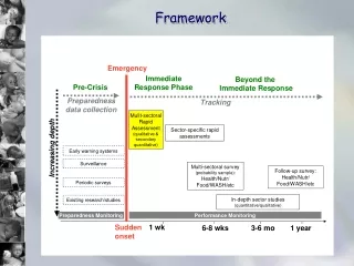
Framework. Upgrade in ATLAS. The upgrade Phase II of the ATLAS Tile Calorimeter implies a complete redesign of the read-out electronics. In order to increase radiation tolerance pipelines, derandomizers and L1 trigger preprocessor will be placed within the off-detector electronics.

E N D
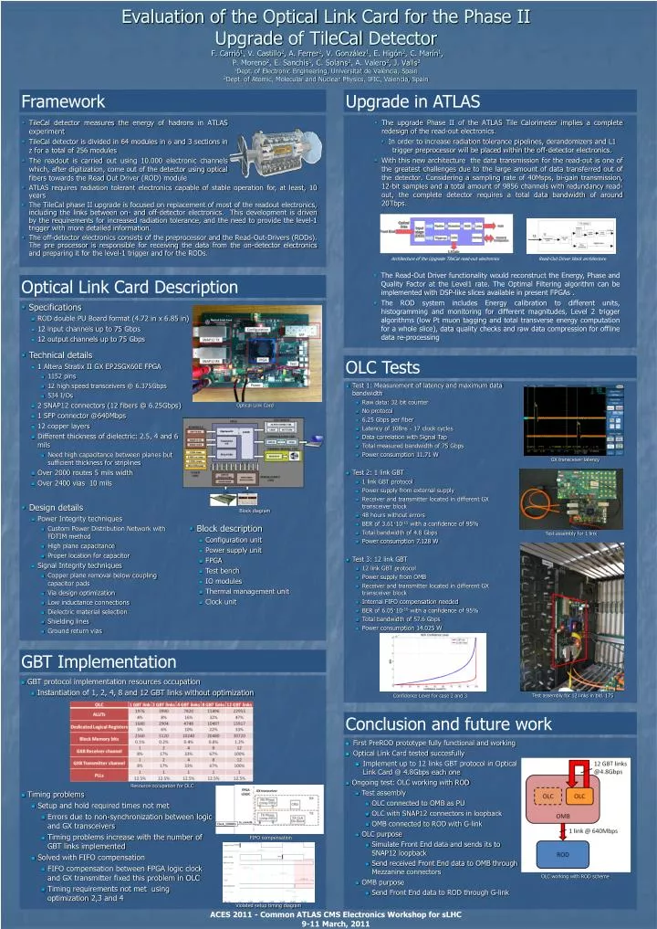
Framework Upgrade in ATLAS • The upgrade Phase II of the ATLAS Tile Calorimeter implies a complete redesign of the read-out electronics. • In order to increase radiation tolerance pipelines, derandomizers and L1 trigger preprocessor will be placed within the off-detector electronics. • With this new architecture the data transmission for the read-out is one of the greatest challenges due to the large amount of data transferred out of the detector. Considering a sampling rate of 40Msps, bi-gain transmission, 12-bit samples and a total amount of 9856 channels with redundancy read-out, the complete detector requires a total data bandwidth of around 20Tbps. • TileCal detector measures the energy of hadrons in ATLAS experiment • TileCal detector is divided in 64 modules in f and 3 sections in z for a total of 256 modules • The readout is carried out using 10.000 electronic channels which, after digitization, come out of the detector using optical fibers towards the Read Out Driver (ROD) module • ATLAS requires radiation tolerant electronics capable of stable operation for, at least, 10 years • The TileCal phase II upgrade is focused on replacement of most of the readout electronics, including the links between on- and off-detector electronics. This development is driven by the requirements for increased radiation tolerance, and the need to provide the level-1 trigger with more detailed information. • The off-detector electronics consists of the preprocessor and the Read-Out-Drivers (RODs). The pre processor is responsible for receiving the data from the on-detector electronics and preparing it for the level-1 trigger and for the RODs. Evaluation of theOptical Link CardforthePhase II Upgrade of TileCal Detector F. Carrió1, V. Castillo2, A. Ferrer2, V. González1, E. Higón2, C. Marín1,P. Moreno2, E. Sanchis1, C. Solans2, A. Valero2, J. Valls21Dept. of ElectronicEngineering, Universitat de València, Spain2Dept. of Atomic, Molecular and Nuclear Physics, IFIC, Valencia, Spain Architecture of the Upgrade TileCal read-out electronics Read-Out Driver block architecture • The Read-Out Driver functionality would reconstruct the Energy, Phase and Quality Factor at the Level1 rate. The Optimal Filtering algorithm can be implemented with DSP-like slices available in present FPGAs . • The ROD system includes Energy calibration to different units, histogramming and monitoring for different magnitudes, Level 2 trigger algorithms (low Pt muon tagging and total transverse energy computation for a whole slice), data quality checks and raw data compression for offline data re-processing Optical Link Card Description • Specifications • ROD double PU Board format (4.72 in x 6.85 in) • 12 input channels up to 75 Gbps • 12 output channels up to 75 Gbps • Technical details • 1 AlteraStratix II GX EP2SGX60E FPGA • 1152 pins • 12 high speed transceivers @ 6.375Gbps • 534 I/Os • 2 SNAP12 connectors (12 fibers @ 6.25Gbps) • 1 SFP connector @640Mbps • 12 copper layers • Different thickness of dielectric: 2.5, 4 and 6 mils • Need high capacitance between planes but sufficient thickness for striplines • Over 2000 routes 5 mils width • Over 2400 vias 10 mils • Design details • Power Integrity techniques • Custom Power Distribution Network with FDTIM method • High plane capacitance • Proper location for capacitor • Signal Integrity techniques • Copper plane removal below coupling capacitor pads • Via design optimization • Low inductance connections • Dielectric material selection • Shielding lines • Ground return vias OLC Tests • Test 1: Measurement of latency and maximum data bandwidth • Raw data: 32 bit counter • No protocol • 6.25 Gbps per fiber • Latency of 108ns - 17 clock cycles • Data correlation with Signal Tap • Total measured bandwidth of 75 Gbps • Power consumption 11.71 W • Test 2: 1 link GBT • 1 link GBT protocol • Power supply from external supply • Receiver and transmitter located in different GX transceiver block • 48 hours without errors • BER of 3.61·10-15 with a confidence of 95% • Total bandwidth of 4.8 Gbps • Power consumption 7.128 W • Test 3: 12 link GBT • 12 link GBT protocol • Power supply from OMB • Receiver and transmitter located in different GX transceiver block • Internal FIFO compensation needed • BER of 6.05·10-16 with a confidence of 95% • Total bandwidth of 57.6 Gbps • Power consumption 14.025 W • Optical Link Card • GX transceiver latency • Block diagram • Block description • Configuration unit • Power supply unit • FPGA • Test bench • IO modules • Thermal management unit • Clock unit • Test assembly for 1 link GBT Implementation • GBT protocol implementation resources occupation • Instantiation of 1, 2, 4, 8 and 12 GBT links without optimization • Test assembly for 12 links in bld. 175 • Confidence Level for case 2 and 3 Conclusion and future work • First PreROD prototype fully functional and working • Optical Link Card tested succesfully • Implement up to 12 links GBT protocol in Optical Link Card @ 4.8Gbps each one • Ongoing test: OLC working with ROD • Test assembly • OLC connected to OMB as PU • OLC with SNAP12 connectors in loopback • OMB connected to ROD with G-link • OLC purpose • Simulate Front End data and sends its to SNAP12 loopback • Send received Front End data to OMB through Mezzanine connectors • OMB purpose • Send Front End data to ROD through G-link • Resource occupation for OLC • Timing problems • Setup and hold required times not met • Errors due to non-synchronization between logic and GX transceivers • Timing problems increase with the number of GBT links implemented • Solved with FIFO compensation • FIFO compensation between FPGA logic clock and GX transmitter fixed this problem in OLC • Timing requirements not met using optimization 2,3 and 4 • FIFO compensation • OLC working with ROD scheme • Violated setup timing diagram ACES 2011 - Common ATLAS CMS Electronics Workshop for sLHC 9-11 March, 2011