Download
1 / 16
180 likes | 420 Views
2011-1 Special Topics in Optical Communications. Reinventing germanium avalanche photodetector for nanophotonic on-chip optical interconnects. Solomon Assefa , Nature, March 2010. Jeong -Min Lee ( minlj@tera.yonsei.ac.kr ) High-Speed Circuits and Systems LAB.

E N D
2011-1 Special Topics in Optical Communications Reinventing germanium avalanche photodetector for nanophotonic on-chip optical interconnects Solomon Assefa, Nature, March 2010 Jeong-Min Lee (minlj@tera.yonsei.ac.kr) High-Speed Circuits and Systems LAB.
2011-1 Special Topics in Optical Communications Contents • Abstract • NanophotonicGe waveguide-integrated APD • Impulse response of an APD • Sensitivity and excess noise measurement • Conclusion High-Speed Circuits and Systems LAB.
2011-1 Special Topics in Optical Communications Abstract • Integration of optical communication circuits directly into high-performance microprocessor chips can enable extremely powerful computer systems. • Ge PD with Si transistor technique:Chip components Infrared optical signals • Capability to detect very-low-power optical signals at very high speed • Suffer from an intolerably high amplification noise characteristic of Ge • Ge layer for detection of light source & Amplification taking place in a separate Si layer High gain with low excess noise Thick semiconductor layer: limit APD speed (10 GHz) with high bias voltages (25 V) High-Speed Circuits and Systems LAB.
2011-1 Special Topics in Optical Communications Abstract • A Ge amplification layer can overcome the intrinsically poor noise characteristics Achieving a dramatic reduction of amplification noise by over 70 % • By generating strongly non-uniform electric fields, the region of impact ionization in Ge(30nm) Noise reduction effects • Smallness APD Avalanche gain: 10 dB (30 GHz, 1.5 V) • Application: Optical interconnects in telecommunications, secure quantum key distribution, and subthresholdultralowpower transistors High-Speed Circuits and Systems LAB.
2011-1 Special Topics in Optical Communications NanophotonicGe waveguide-integrated APD • For on-chip interconnects, the germanium(Ge)-based APD photodetector should be integrated into a silicon waveguide that can route near-infrared light on a silicon chip. • Ideal APD:Compact micrometer-scale foot print, operate at a 1V Compatible with CMOS technology, high avalanche gain, detect very fast optical signals of up to 40 Gbps. Contradiction & Innovation • A waveguide-integrated Ge APD • Thickness and width of both Ge and Si layers were optimized to ensure the highest responsibility • Thickness: Ge (140 nm), Si (100 nm) • Width: Ge (750 nm), Si (550 nm) High-Speed Circuits and Systems LAB.
2011-1 Special Topics in Optical Communications NanophotonicGe waveguide-integrated APD • Provide propagation of at most only two optical modes in the combined layer stack for the transverse electric field polarization at both the 1.3 & 1.5 um wavelenghts. • Allows efficient coupling of light from the routeing silicon waveguide • The resulting optical power resides almost completely in top Ge layer (77%) • Short absorption length (10um) minimize the APD capacitance (10 fF) High-Speed Circuits and Systems LAB.
2011-1 Special Topics in Optical Communications NanophotonicGe waveguide-integrated APD • Problem: Growth of such a thin Ge layer directly on top of Si using epitaxial technique Large concentration of misfit dislocations • Solution: Rapid melting growth technique (Si – SiON – Ge) High-Speed Circuits and Systems LAB.
2011-1 Special Topics in Optical Communications NanophotonicGe waveguide-integrated APD • Very thin Ge layer Ensure fast operation up to 40 Gbps • Cu – W – Ge: W plugs are in direct contact with the Ge layer A series of metal-semiconductor-metal Schottky diode Strong electric fields (30 kVcm-1) in small thickness of Ge (2.8 V) • High E fast acceleration of both electrons and holes to their saturation velocities • Complete electrical isolation block unwanted slow diffusion of photo-generated carriers fast response High-Speed Circuits and Systems LAB.
2011-1 Special Topics in Optical Communications Impulse response of an APD • Total area under the impulse response total # of carriers collected at the electrodes • 0.5 ~ 1.5 V flat: all photo-generated carriers are being collected • R = 0.4 A/W (1.3 um) • R = 0.14 A/W (1.5 um) • Exponential increase: A significant current gain (M = 10 @ 3.5 V) • Over 1 V: fast component makes up 70% of the pulse area Gain is fast & broadband (inset of Fig.2b) High-Speed Circuits and Systems LAB.
2011-1 Special Topics in Optical Communications Impulse response of an APD • Avalanche gain origin: • p-i-n: uniform E distribution MSM contact: non-uniform fields (red: exceeds 120 kVcm-1) high probability of impact ionization • A series of small-signal radio-frequency measurements: • 10 MHz ~ 1 GHz: flat frequency response • (Fig.3a) 3 dB BW: 5 ~ 34 GHz (0.1 ~ 1.1 V) High-Speed Circuits and Systems LAB.
2011-1 Special Topics in Optical Communications Impulse response of an APD • (Fig.3d) Gain flat btw 0.4 ~ 0.8 V collection of all photo-generated carriers • Similar high M but higher voltages around 3.7 V • Higher bias BW constant (carriers reach their saturation velocity) • However, gain x bandwidth continues to grow (because of rise in avalanche gain) 300 GHz • Saturation of the bandwidth before considerable gain is reached carrier transport and avalanche amplification are taking place in spatially separated areas within the APD • Red : 200 nm contact spacing • Blue: 400 nm contact spacing High-Speed Circuits and Systems LAB.
Sensitivity and excess noise measurement • A large (10 dB) avalanche gain in the APD does not necessarily guarantee a corresponding increase in the detector sensitivity Can easily degrade as a result of the higher excess noise level (Fig.4a) sensitivity continues to improve even after the unity gain plateau is reached, at around 0.7 V High-Speed Circuits and Systems LAB.
Sensitivity and excess noise measurement • (Fig.4b) Improvement of sensitivity measured at a BER of 10-9. • Sensitivity: -8 dBm(Absolute) A significant improvement of 5.9 dB at a bias of 3.2 V was achieved (Gain: 11.8 dB) • High dark current main factor resulting in saturation of sensitivity improvement (50 uA @ a unity gain) • Keff= 0.1 Improvement in sensitivity of over 10 dB @ 40 Gbps can be expect that dark current could be suppressed 10 times High-Speed Circuits and Systems LAB.
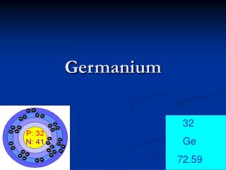
Sensitivity and excess noise measurement • Keff: effective ratio of ionization coefficient for electrons and holes almost equal in bulk Ge (keff= 0.9) large excess noise conventional Ge APD uncompetitive for building digital optical links • Total reduction of noise can be estimated as more than 70% wrt the noise expected for a bulk Ge High-Speed Circuits and Systems LAB.
2011-1 Special Topics in Optical Communications Conclusion • Several factors can account for the dramatic reduction of excess multiplication noise in our nanophotonic APD • The avalanche multiplication is happening only in very close proximity to the W plug (30 nm) Thinning the multiplication region excess noise reduce • Initial energy effect carriers entering the multiplication region have already acquired high energy narrow the probability distribution functions and suppress excess multiplication noise • The large electric field gradients further narrowing of the probability distribution functions owing to the fast acceleration of secondary carriers towards the ionization threshold. High-Speed Circuits and Systems LAB.
2011-1 Special Topics in Optical Communications Thank you for listening Jeong-Min Lee (minlj@tera.yonsei.ac.kr) High-Speed Circuits and Systems