Download
1 / 20
200 likes | 324 Views
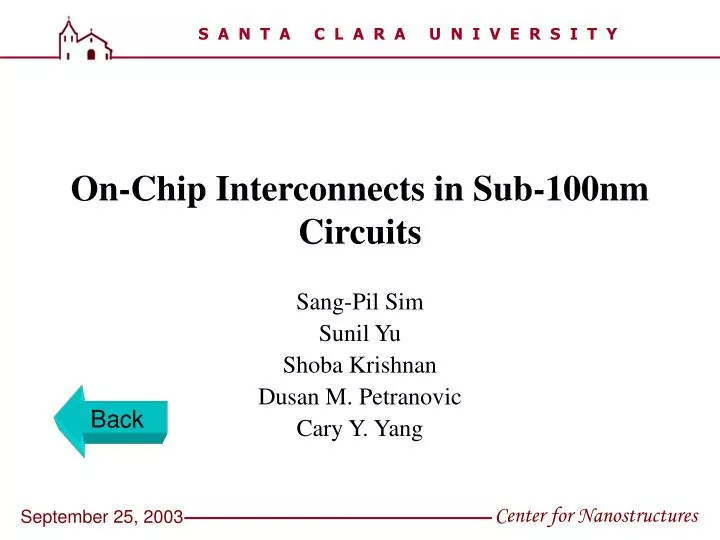
On-Chip Interconnects in Sub-100nm Circuits. Sang-Pil Sim Sunil Yu Shoba Krishnan Dusan M. Petranovic Cary Y. Yang. Back. Motivation Effective Loop Inductance High Frequency Effects Frequency-Dependent RLC Model Non-Orthogonal Wires Conclusion. Outline.

E N D
On-Chip Interconnects in Sub-100nm Circuits Sang-Pil Sim Sunil Yu Shoba Krishnan Dusan M. Petranovic Cary Y. Yang Back
Motivation • Effective Loop Inductance • High Frequency Effects • Frequency-Dependent RLC Model • Non-Orthogonal Wires • Conclusion Outline
On-Chip Inductance (I) • Increases wire delay and worsens signal integrity when • As technology advances, more wires will show inductive behavior • Accurate RLC model is imperative for optimal design of today’s ULSI systems Gate delay (tr) < RC Wire delay (RCl2) < 2* flight time (2 l)
Finding return path is not straightforward • Partial inductance methodology alleviate the problem with a hypothetical return path On-Chip Inductance (II) I Mutual Inductance Self Inductance
Motivation • Partial inductance methodology is not appropriate for large circuits or full chip • For multi-GHz freq., return current through capacitive coupling should be considered • Non-orthogonal wires are being utilized • Effective loop inductance model for general high-frequency non-orthogonal wires becomes necessary
Power grid: designated ground line • Random lines: capacitive coupling path High-Freq. Digital Interconnect
LF : Low resistance path • MF : Low inductance path • HF : Low inductance by capacitive coupling Reff and Leff versus Frequency Return path is determined by R L L & C
Given by partial inductance and resistance • Frequency-dependent Loop Inductance and Resistance
Reff & Leff show sufficient linearity for hierarchical model construction Foundation - Linearity S=3mm & P=40mm
Slight under-estimation of L at LF is caused by super-linearity Comparison with Field-Solver Line – model, Symbol – FastHenry (10mm, 300mm) (20mm, 365mm) P=40mm (5mm, 340mm)
Slight under-estimation of LLF does not change overall impedance characteristics of wire • Analytic & hierarchical model construction is validated for power grid configuration Effect of Super-Linearity in LLF
Full-wave simulation (0.1 to 100GHz) • RLCG extraction from the resulting S-parameters • Random lines are left floating High-Frequency Effect
Full Wave Full Wave (random lines) G G S G G 2 10 10 2 3 2 3 2 10 10 Effect of Random Signal Lines
Q-TEM mode approximation using SWFs at HF • Separate SWFs for parallel and crossing lines • Inductance extraction from capacitance Correlation between L and C
Reff() C Leff() Freq-Dependent RLC Model Freq. Reff Leff Extraction Low from power grid, using energy equivalence Medium High from C, empirically
G G S G G 2 10 10 2 3 2 3 2 10 10 Comparison with Field Solver
Diagonal Wires • Can be modeled by an equivalent orthogonal power grid • Same SWF as orthogonal is observed S = 3, 5, 10, 15, 20, 25mm, and P=50mm
Conclusion • Analytic and hierarchical construction of loop inductance is verified for power grid configuration • Random signal line effect is quantitatively investigated, leading to an empirical model • The wide-band characteristics of on-chip wire are incorporated into RLC circuit valid up to 100GHz • Non-orthogonal architecture can be included into the proposed model
Partners • Cadence Design Systems - Dr. N. Arora • Intel - Dr. C. Dai • KAIST - Prof. K. Lee Publications Sang-Pil Sim, et al., “An effective loop inductance model for general non-orthogonal interconnect with random capacitive coupling,” Technical Digest of IEDM, pp. 315-318, Dec. 2002. Sang-Pil Sim, et al., “High-frequency on-chip inductance model,” IEEE Electron Device Letters, vol. 33, pp.740-742, Dec. 2002. Sang-Pil Sim, et al., “A Unified RLC Model for High-Speed On-Chip interconnects,” IEEE Trans. on Electron Devices, vol. 50, p.1501, Jun. 2003.