Download
1 / 33
470 likes | 909 Views
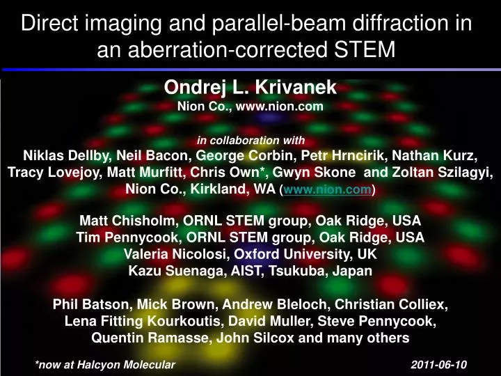
Direct imaging and parallel-beam diffraction in an aberration-corrected STEM. Ondrej L. Krivanek Nion Co., www.nion.com in collaboration with Niklas Dellby, Neil Bacon, George Corbin, Petr Hrncirik, Nathan Kurz, Tracy Lovejoy, Matt Murfitt, Chris Own*, Gwyn Skone and Zoltan Szilagyi,

E N D
Direct imaging and parallel-beam diffraction in an aberration-corrected STEM Ondrej L. Krivanek Nion Co., www.nion.com in collaboration with Niklas Dellby, Neil Bacon, George Corbin, Petr Hrncirik, Nathan Kurz, Tracy Lovejoy, Matt Murfitt, Chris Own*, Gwyn Skone and Zoltan Szilagyi, Nion Co., Kirkland, WA (www.nion.com) Matt Chisholm, ORNL STEM group, Oak Ridge, USA Tim Pennycook, ORNL STEM group, Oak Ridge, USA Valeria Nicolosi, Oxford University, UK Kazu Suenaga, AIST, Tsukuba, Japan Phil Batson, Mick Brown, Andrew Bleloch, Christian Colliex, Lena Fitting Kourkoutis, David Muller, Steve Pennycook, Quentin Ramasse, John Silcox and many others *now at Halcyon Molecular 2011-06-10
Washington state, USA: 1st EM outside of Europe… Washington state EM history continued: 1997 - Krivanek and Dellby report on the first working (S)TEM aberration corrector: Inst. Phys. Conf. Ser. 153 (Proceedings 1997 EMAG meeting) p. 35. 2000 - Nion delivers the first commercial electron-optical aberration corrector in the world; corrector attains <1 Å directly interpretable resolution in 2001 (Nature 418, 617). 2010 - Nion delivers its first complete electron microscope (a 200 kV STEM) …and now the place of origin of the most recent STEM in the world
Main topics Part I Scanning transmission electron microscopy: an overview Aberration correction: why is it important? Nion UltraSTEM construction and performance Imaging and elemental mapping Part II Parallel-beam diffraction in the STEM: the pre-requisites
STEM, an instrument for imaging, analysis and diffraction • Scanning Transmission Electron Microscope (STEM): • make a small + intense electron probe, detect and quanti-tativelymeasure all the signals that come off the sample. • An aberration-corrected STEM uses sophisticated electron optics (with ~ 100 independent elements) to produce a very small electron probe, down to ~0.5 Å Ø. • Three signals are especially interesting: • High–angle (Rutherford-scattered) electrons: >90 mr scattering from atomic nuclei, collected as a mostly incoherent signal by a high angle annular dark field detector (HAADF), to show where are the atoms, 2) Inelastically-scattered electrons: scattered by the sample’s electrons, collected and analyzed by an electron energy-loss spectrometer (EELS), they show what type the atoms are, and other sample properties), • 3) Low+medium-angle scattered electrons: collected by a medium-angle detector (MAADF) or a CCD camera, as a mostly coherent signal, they reveal the crystal structure. schematic is from: Focus on improving transmission electron microscopes starts to pay off, Physics Today, June 2010, pp. 15-19 more info at: http://www.nion.com/resources.html
Why is aberration correction important? Aberration-corrected space telescope: a revolution in astronomy After repair: spherical aberration of telescope’s mirror is corrected by newly designed planetary camera optics. Hubble space telescope, before repair. Image is blurred by spherical aberration of incorrectly made primary mirror.
Si N Si Aberration correction: a revolution in electron microscopy Graphene before and after aberration correction Aberration-corrected annular dark field image, Nion UltraSTEM, 60 kV Matt Chisholm, ORNL (2010) Individual atoms are clearly visible, and their type can be distinguished by their image intensity. Uncorrected bright field phase contrast image, JEOL 2010F, 120 kV Nature 430 (2004) 870-873 (Fig. 2b) Image is blurred by the spherical aberration of the objective lens: individual atoms cannot be seen.
C1,0 C1,2 C2,1 C2,3 C3,0 C3,2 C3,4 C4,1 C4,3 C4,5 C5,0 C5,2 C5,4 C5,6 Nion 3rd generation spherical aberration corrector • 16 quadrupole and 3 quadrupole/ octupole stages: 19 layers total • carefully managed axial and field trajectories • designed to correct Cs (a.k.a. C3) while giving only 0.1 mm increase in Cc, to set all C5’s to 0 (including C5,6), and to give minimized C7’s • bakeable to 140 C and UHV-compatible corrected (or minimized) aberrations The resultant optical instrument needs autotuning and other diagnostic methods so that it can be set up automatically by computers.
STEM probe size in the aberration-corrected era Graph shows probe size for probe current Ip = 0.25 Ic Ic = coherent probe current (~0.1-1 nA for CFEG) uncorrected STEM, Cs = 1 mm Resolution reached in the Nion 200 keV column For the expressions describing the above curves, see Krivanek et al.’s chapter in the just-published Pennycook-Nellist STEM volume (Springer).
Nion UltraSTEM™ 200 Fully modular and thus very flexible true UHV at the sample (~5x10⁻¹⁰ torr) ultra-precise stage with 0.5 nm minimum mechanical motion computer-controlled sample exchange 3rd and 5th order correction for probe 3rd order aberration correction for EELS Ultra-stable (probe jitter <0.1 Å rms) Aberration corrector 2 Aberration corrector 1 Described in: Krivanek et al. Ultramicroscopy 108 (2008) 179-195 and Dellby et al. EPJAP in press. More info at www.nion.com. instrument shown: CNRS Orsay, France
200 kV UltraSTEM: new CFEG & EELS ZL peaks The gun is a three-part design: the HT generation the HT measurement, the beam acceleration are done in separate volumes. This makes it possible to stabilize the HT more effectively. The gun accelerates the electrons as rapidly as possible, using a shortened accelerator. This minimizes electron-electron Coulomb interactions (Boersch effect) and gives less energy spread and higher gun brightness at useful emission currents. It is designed to operate at any kV between 20 and 200.
200 kV imaging of a gold particle at low current Making sure the small spacing reflections are real: rotate the scan direction and record the image again. HAADF image and FFT of a gold particle. UltraSTEM200, 200 kV, 15 pA beam current.
(0.123 nm) -1 Resolving 1.23 Å at 40 keV HAADF image and FFT of a gold particle at 40 kV. Nion UltraSTEM200, 60 pA beam current. Second zone operation of a 4 mm gap objective lens: the optical properties approximate those of a 2 mm gap OL.
Real-space crystallography: MAADF STEM of graphene Medium-angle annular dark field (MAADF) STEM imaging gives about 1.1 Å resolution at 60 kV (below the knock-on threshold), and is very quantitative. Images become clearer if they are Fourier-filtered to remove high frequency shot noise and probe tails. Image intensity scales as ~Z1.64 Krivanek et al. Ultramicroscopy 110 (2010) 935-945 raw data processed
Carbon nanotube imaged at 60 keV MADF image of single wall carbon nanotube, Nion UltraSTEM100. Masking a set of reflections in the FFT allows the front and the back of the nanotube to be visualized separately. Image courtesy Matt Chisholm, ORNL. dose ~ 109 e- / nm2 Microscope is housed in a soft steel box, shown here with one of its side doors open. The box makes the microscope relatively insensitive to external disturbances. It also serves as a bake-out enclosure.
Atom-by-atom crystallography I: single layer BN, with O and C impurities 1.4 Å 60 kV MAADF image B and N atoms are readily identifiable by their MAADF intensities. C and O substitutional impurities are also identifiable in the line profiles.
BN monolayer with impurities: histogram analysis Histogram analysis of image shows that B, C, N and O can be identified unambiguously in monolayer BN. The experimentally worked out dependence of image intensity on Z goes as Z1.64. Nature 464 (2010), 571-574. Dose required: ~107 e- / Å2
Result of DFT calculation overlaid on the experimental image C ring is deformed N Cx6 B O Longer bonds Na adatom BN monolayer with impurities: the final result C O C
Atom-by-atom crystallography II: Si and N in graphene Si 5 5 Si Si (5x) 9 7 Si N 5 5 5 7 Si and N at and near topological defects (rings other than 6-fold are labeled, note that net departure from 6-fold = 0) Si in topologically correct graphene (but with longer Si-C bonds than C-C bonds) Si at graphene’s edge MAADF images of graphene. Nion UltraSTEM100, 60 kV. Image courtesy Matt Chisholm, ORNL, sample courtesy V. Krisnan and G. Duscher, U. of Tennessee
Species-sensitive crystallography: EEL spectrum from 3 Er atoms, and Spectrum-Images HAADF image MAADF Spectrum-images Single Er atoms 1.4 nm Er-N4,5 C-K Er-N4,5 C-K C Er The size of the atoms in the Er N4,5 image is only about 3 Å, and nanopods can be seen in the C map Dose required: ~108 - 109 e- / Å2
EELS atomic-resolution chemical mapping (2007) La0.7Sr0.3MnO3/SrTiO3 multilayer 40 mr illum. half-angle 0.4 nA beam current ~1.2 Å probe >70% efficiency EELS coupling 64x64 pixel map 7 msec per pixel, i.e. 29 sec total acquisition time 10 sec additional processing time i.e., <1 min total time Nion UltraSTEM100, 100 keV La (M) Ti (L) RGB Mn (L) 5 Å Muller et al., Science 319, 1073–1076 (2008)
Imaging different chemical species separately Imaging of oxygen octahedral rotations in LaMnO3. Nion Ultra-STEM100, Gatan Enfina EELS, 100 keV. Courtesy Maria Varela and Steve Pennycook, ORNL. 1 nm 1 nm O-K Mn-L2,3 La-M4,5 RGB composite
Mapping atomic bonding in EuTiO3/DyScO3 Increased Eu valence is found in a single atomic layer at the interface. Nion UltraSTEM100, 100 kV. Courtesy Lena Fitting-Kourkoutis and David Muller, Cornell U. Proceedings IMC17. Eu2+ Eu3+ Eu elemental map showing a reduced Eu concentration at the interface Three-component fit to the full SI demonstrating 2D mapping of bonding changes with atomic resolution Evolution of the horizontally averaged Eu-M edge fine structure across the interface Part of simul-taneously recorded HAADF image The three components extracted using MCR methods
Part II: classical (reciprocal space) crystallography in the STEM Two possibilities for recording reciprocal space data: 1) Leave the beam as it is set up for imaging, record and analyze convergent beam diffraction patterns. Depending on how the illumination (and the sample) are set up, the patterns can be either coherent (fringes are seen in Bragg disk overlap regions) or incoherent (no fringes). 2) Make the beam parallel, record and analyze point-like diffraction patterns.
Convergent beam to nanodiffraction: one mouse-click Coherent convergent-beam diffraction pattern (Ronchigram) With aberration correction, the fringes are straight. Parallel-beam diffraction pattern from the same [110] Si sample area (=nanodiffraction 1) Going from one mode to the other takes about 3 s, the probe stays on the same area.
Going from a convergent to a parallel probe in the STEM Changing the beam conver-gence is done very simply, by changing the focal lengths of the condenser lenses. Two types of trajectories are needed to understand the optics: axial and field Conservation of brightness means that: crossover size times angular range = constant beam direction Note that tracing out the field trajectories shows that the image of aperture moves around when the magnification is changed source magnified 0.5x, angular range magnified 2x source magnified 2x, angular range magnified 0.5x Axial trajectories cross the axis in the image (and object) planes, field trajectories traverse the image plane away from the optic axis, and cross the axis at the angular range-defining aperture.
Two types of principal planes in the illumination column The two planes: A – image of source B – focused image of aperture alternate throughout the illumination column. (similar to the way image and diffraction planes alternate in an imaging column) Either plane can be projected onto the sample as the illumination. A is typically used for forming small probes, B for broad, Köhler-type illumination. image of source image of aperture mixed image image of source image of aperture (sin(x) /x)2 In all other planes, there is a de-focused image of the aperture. image of source
Practical implementation scattered electrons BFP sample A (source image): ~50x demagnifi- cation by the obje-ctive lens gives: source size projected onto the sample: <0.1 nm convergence semi-angle: > 30 mr B (Köhler ill.): beam semi-angle at sample: ao = dffp / 2fo convergence semi-angles 0.1-0.01 mr are easily obtained (= 40 nm / (2x2mm)) Probe size at sample is then: dp = 0.61 l / ao =200 nm - 2 µm BFP OL scan coils fo FFP FFP corrector beam direction C3 C2 crossover size in condenser section ~ few nm convergence ~ 1 mr aperture C1 CFEG source size ~ 3nm CFEG convergent beam microdiffraction
Five practical ways of illuminating the sample in STEM beam direction regular imaging mode (±30 mr) change to 1 mr semi-angle 1 mr semi-angle using mini-lens 0.1 mr semi-angle, OL on 0.1 mr semi-angle, OL off
Probe size vs. convergence angle diffraction-limited probe diameter: The above is only valid with zero source size, i.e. zero beam current. For non-zero probe currents, the probe size broadens as: Ip … probe current Ic … coherent current (of the source) if Ip = Ic , dp = √2 dd
Coherent probe current The coherent current is a characteristic property of the source. It is independent of the accelerating voltage, aberrations and aperture size used. Its value is related to normalized (reduced) brightness Bn as: when Ip < Ic, the probe can be said to be largely coherent when Ip > Ic, the probe is largely incoherent Some typical Ic values: Ic (pA)Bn (A/ (m2 sr V) cold field emission (CFE): 150-500 1-3 x 10⁸ Schottky guns: 30-150 0.2-1 x 10⁸ LaB6 guns: ~1 ~106 (more detailed explanation, including a discussion of why Schottky guns should not be called FEGs, is in Krivanek et al.’s chapter in the Pennycook-Nellist STEM book)
Three ways of scanning/rocking the beam in the STEM beam direction scanned probe moves on the sample nearly parallel-like, but not quite without Cs compensation, probe rocking works best for angles < 20 mr with Cs compensation, >50 mr should be possible
Compensated rocking: 3 ingredients needed 1) Complete scan-descan coil system, preferably symmetric about the OL. 2) Electronics control which makes the currents supplied to the 4 layers of scan coils completely programmable. 3) Software that computes and implements the scan ramps required for compensated beam rocking. (1+2) are available in the Nion UltraSTEM column. (2) is implemented by pre-computing a table of deflections to be done by all the scan layers, and then reading it out and implementing it at pixel advance rates of up to 1 pixel / 50 µs (=20k scan points per second). (3) has not been done yet. It consists of computing the required scans and loading them into the computer memory. Interested students please see me.
Conclusions • The STEM is a very flexible instrument (but some STEMs are more flexible than others). • Imaging single atoms is not difficult with an aberration-corrected STEM. It’s also possible to identify the type of the individual atoms, by ADF imaging, EELS, and also EDXS. • Parallel-beam difraction with nm-sized coherent probes in the STEM promises to be very powerful, but it has not yet been fully explored. • The full power of the new techniques is yet to be applied across the whole of physics, materials science and biology. • An Erice school on aberration-corrected (S)TEM might be a very good idea!