Download
1 / 1
10 likes | 138 Views
GaN nanorods grown on Si (111) substrate by Plasma-Assisted Molecular Beam Epitaxy. I. Abstract. II. Experiments. III. Results and discussion. Sample A (T S =780 ℃ ). Sample B (T S =790 ℃). Sample C (T S =790 ℃). Sample D (T S =790 ℃). 500 nm n-GaN. 500 nm n-GaN. Growth direction.

E N D
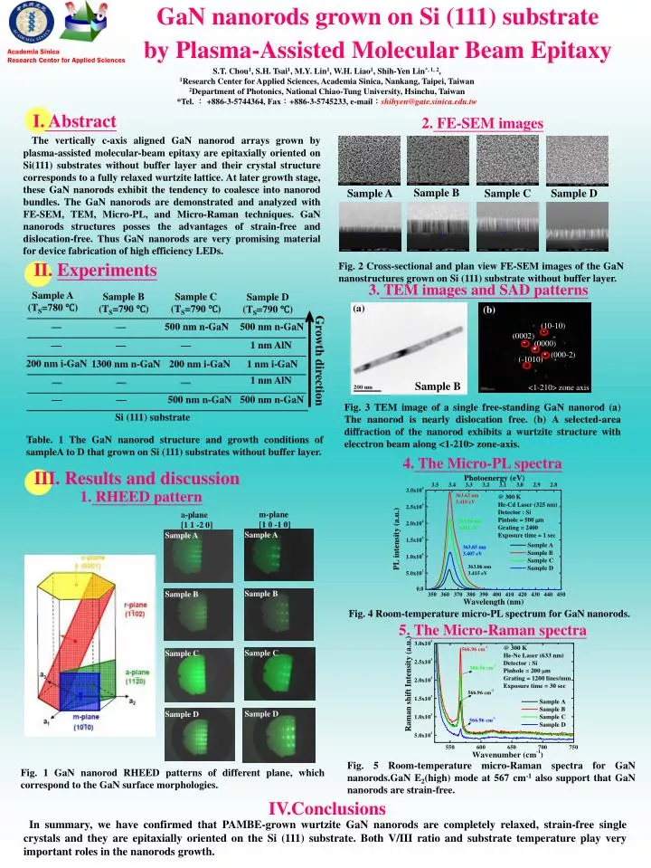
GaN nanorods grown on Si (111) substrate by Plasma-Assisted Molecular Beam Epitaxy I. Abstract II. Experiments III. Results and discussion Sample A (TS=780 ℃) Sample B (TS=790 ℃) Sample C (TS=790 ℃) Sample D (TS=790 ℃) 500 nm n-GaN 500 nm n-GaN Growth direction 1 nm AlN 200 nm i-GaN 1300 nm n-GaN 200 nm i-GaN 1 nm i-GaN 1 nm AlN 500 nm n-GaN 500 nm n-GaN Si (111) substrate Academia Sinica Research Center for Applied Sciences S.T. Chou1, S.H. Tsai1, M.Y. Lin1, W.H. Liao1, Shih-Yen Lin*, 1, 2, 1Research Center for Applied Sciences, Academia Sinica, Nankang, Taipei, Taiwan 2Department of Photonics, National Chiao-Tung University, Hsinchu, Taiwan *Tel. : +886-3-5744364, Fax:+886-3-5745233, e-mail:shihyen@gate.sinica.edu.tw 2. FE-SEM images The vertically c-axis aligned GaN nanorod arrays grown by plasma-assisted molecular-beam epitaxy are epitaxially oriented on Si(111) substrates without buffer layer and their crystal structure corresponds to a fully relaxed wurtzite lattice. At later growth stage, these GaN nanorods exhibit the tendency to coalesce into nanorod bundles. The GaN nanorods are demonstrated and analyzed with FE-SEM, TEM, Micro-PL, and Micro-Raman techniques. GaN nanorods structures posses the advantages of strain-free and dislocation-free. Thus GaN nanorods are very promising material for device fabrication of high efficiency LEDs. Sample B Sample A Sample C Sample D Fig. 2 Cross-sectional and plan view FE-SEM images of the GaN nanostructures grown on Si (111) substrate without buffer layer. 3. TEM images and SAD patterns (a) (b) (10-10) (0002) (0000) (000-2) (-1010) <1-210> zone axis Sample B Fig. 3 TEM image of a single free-standing GaN nanorod (a) The nanorod is nearly dislocation free. (b) A selected-area diffraction of the nanorod exhibits a wurtzite structure with elecctron beam along <1-210> zone-axis. Table. 1 The GaN nanorod structure and growth conditions of sampleA to D that grown on Si (111) substrates without buffer layer. 4. The Micro-PL spectra 1. RHEED pattern m-plane [1 0 -1 0] a-plane [1 1 -2 0] Sample A Sample A Sample B Sample B Fig. 4 Room-temperature micro-PL spectrum for GaN nanorods. 5. The Micro-Raman spectra Sample C Sample C Sample D Sample D Fig. 5 Room-temperature micro-Raman spectra for GaN nanorods.GaN E2(high) mode at 567 cm-1 also support that GaN nanorods are strain-free. Fig. 1 GaN nanorod RHEED patterns of different plane, which correspond to the GaN surface morphologies. IV.Conclusions In summary, we have confirmed that PAMBE-grown wurtzite GaN nanorods are completely relaxed, strain-free single crystals and they are epitaxially oriented on the Si (111) substrate. Both V/III ratio and substrate temperature play very important roles in the nanorods growth.