Download
1 / 35
470 likes | 857 Views
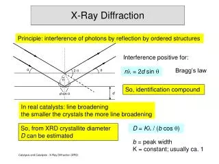
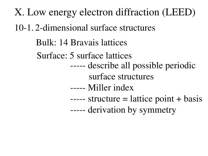
X. Low energy electron diffraction (LEED). 10-1. 2-dimensional surface structures. Bulk: 14 Bravais lattices. Surface: 5 surface lattices. ----- describe all possible periodic surface structures ----- Miller index ----- structure = lattice point + basis

E N D
X. Low energy electron diffraction (LEED) 10-1. 2-dimensional surface structures Bulk: 14 Bravais lattices Surface: 5 surface lattices ----- describe all possible periodic surface structures ----- Miller index ----- structure = lattice point + basis ----- derivation by symmetry
(a) Rectangular lattice (a b, = 90o) (b) Centered rectangular lattice (a b, = 90o)
(c) Parallelogram (oblique) lattice (a b, 90o) (d) square lattice(a= b, = 90o)
(e) Hexagonal lattice(a= b, = 120o) We have shown that there are only five plane lattices in Chapter 3-1. Example: The ideal Si(111) surface: a hexagonal lattice. The ideal Si(100) surface: a square lattice. The (110) surface of Au: a rectangular lattice. FCC
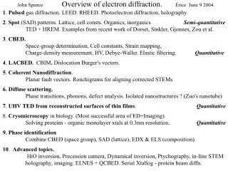
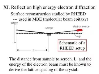
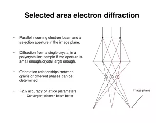
10-2. Techniques for surface structure determination • LEED (Low energy electron diffraction) • RHEED (Reflection high energy electron • diffraction) • STM (Scanning tunneling microscope) • SEXAFS (Surface extended X-ray • absorption fine structure) In this course, LEED and RHEED will be covered.
http://www.omicron.de/cache/media_GB_IMG_0093C_freigestellt%5B2467%5D_20111208-122653_omicronmedia_image_paddedthumbnailscheme_ffffff_800x1200.jpghttp://www.omicron.de/cache/media_GB_IMG_0093C_freigestellt%5B2467%5D_20111208-122653_omicronmedia_image_paddedthumbnailscheme_ffffff_800x1200.jpg
Electron escape depth and surface sensitivity http://www.globalsino.com/micro/TEM/images/TEM9923.gif
The reciprocal lattice of the surface in LEED Total scattering amplitude F for LEED is : the electron density in the volume that electrons are scattered and collected in the detector (screen).
In LEED, electrons are diffracted from volume within electron escape depth. If the electron beam size is 100 nm and the escape depth is 0.5 nm, the volume is in a disk shape.
10-3.Ewald sphere construction the Si(100) ideal surface in LEED The atomic structure of the Si(100) ideal surface -110 110
However, the LEED pattern of as-cleaned Si(100) is not a square lattice The LEED pattern for the Si(100) surface cleaned at 950 is double domain Si(100)-2x1 shown below, rather than Si(100)1x1
Explain this pattern later! http://upload.wikimedia.org/wikipedia/en/thumb/c/c4/Si100Reconstructed.png/639px-Si100Reconstructed.png
> LEED using different electron kinetic energies 10 10 2B <2B kinetic energy of electron increases k radius of Ewald sphere diffracted spots move inwards the sreeen
Low E High E
III. Surface reconstruction (defined in the real space) (a) For a reconstructed surface Wood’s notation Where M is the chemical element, (hkl) is the plane, Ris the rotation angle between the axes of surface and bulk
For example: Si(100)2x1 LEED pattern of single domain Si(100)2x1
Another domain Supposition of two domain double domain of Si(100)2x1
Si(111) surface reconstructions and their LEED patterns Question • What are the reciprocal lattices of the Si(111)1x1, Si(111)2x1, and Si(111)7x7 surfaces? • What are the LEED patterns of the Si(111)1x1, Si(111)2x1, and Si(111)7x7 surfaces?
Picture from the NIST Surface Structure Database Si(111)1x1 http://www.fhi-berlin.mpg.de/KHsoftware/Balsac/BalsacPictures/SSDfig99.gif
Si(111)2x1 http://www.fhi-berlin.mpg.de/KHsoftware/Balsac/BalsacPictures/SSDfig89.gif
Si(111)7x7 http://www.fhi-berlin.mpg.de/KHsoftware/Balsac/BalsacPictures/SSDfig91.gif
Practice for wood’s notation: http://www.chem.qmul.ac.uk/surfaces/scc/scat6_4.htm http://www.chem.qmul.ac.uk/surfaces/scc/scat6_1.htm
100 1x2
100 110 2x2 2x2
100 110 c2x2 c2x2
Substrate: fcc (111) Substrate unit cell 2x2 Surface or abrorbate unit cell
Substrate: fcc (111)
10-5.Adsorbate surface structure For an adsorbate surface Where M is the chemical element, (hkl) is the plane, R is the rotation angle between the axes of surface and bulk, and A is the adsorbate.