Download
1 / 22
220 likes | 390 Views
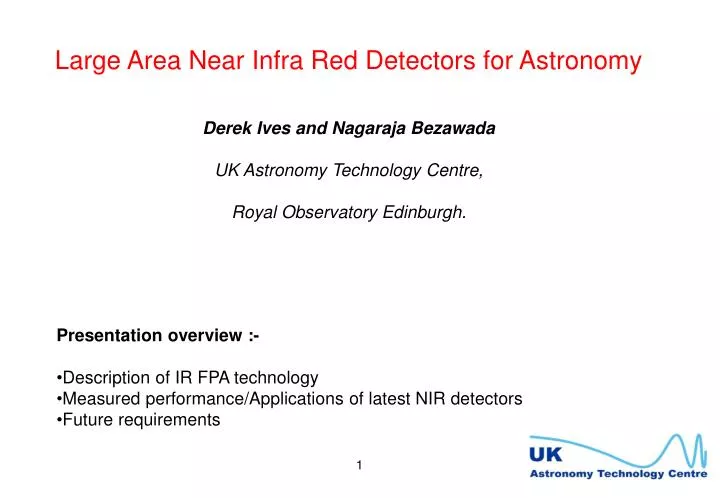
Large Area Near Infra Red Detectors for Astronomy Derek Ives and Nagaraja Bezawada UK Astronomy Technology Centre, Royal Observatory Edinburgh. Presentation overview :- Description of IR FPA technology Measured performance/Applications of latest NIR detectors Future requirements.

E N D
Large Area Near Infra Red Detectors for Astronomy Derek Ives and Nagaraja Bezawada UK Astronomy Technology Centre, Royal Observatory Edinburgh. • Presentation overview :- • Description of IR FPA technology • Measured performance/Applications of latest NIR detectors • Future requirements 1
Large Area Infra Red Detectors for Astronomy • SWIR –> 1-2.5 µm • 2048 x 2048 pixels, typically 18-20 µm2 • Low background • Low Noise ~ 15e • 16/32 outputs =>1 Hz frame rates • NIR –> 1-5 µm • 1024 x 1024 pixels, typically 18-27 µm2 • Low Noise ~ 50e • 32 outputs =>10 Hz frame rates VIRGO 2k x 2k NIR detector • MIR –> 5-25 µm • 320 x 240 pixels, typically 30-50 µm2 • Big well/High background • 16 outputs =>100 - 500 Hz frame rates 2
Si PIN InGaAs SWIR HgCdTe MWIR HgCdTe InSb LWIR HgCdTe Si:As IBC Temperature and wavelengths of high performance detector materials. Approximate detector temperatures for dark currents << 1 e-/sec 3
IRFPA Manufacturing Process Silicon Multiplexer • The HgCdTe wafers are prepared by first growing a thin buffer layer of CdTe on the sapphire substrate(effective first order AR coating for HgCdTe) by metal organic chemical vapor deposition (MOCVD). The photosensitive HgCdTe is then grown via liquid phase epitaxy (LPE) from a Te—rich melt on to the buffered sapphire substrates to produce 2" or 3" HgCdTe wafers. • The photovoltaic detectors are formed by boron ion implantation at room temperature followed by annealing. The detector architecture here is n-on-p. • The junctions are passivated by ZnS or CdTe. • Metal pad deposition for contact to the junction and ground. • Indium columns are evaporated to provide interconnects for subsequent hybrid mating. Indium Metal ZnS passivation n type HgCdTe p-type HgCdTe CdTe Sapphire substrate Newer production methods - Molecular Beam Epitaxy HgCdTe on CdZnTe Lattice matching/lower defect densities => lower dark current 4
IR detector hybridised to Silicon Multiplexer Circuit Detector Array Indium bumps Flip chip bonding ! Silicon Readout Integrated Circuit (ROIC) Over 4,000,000 indium bumps per detector ! • MUX features :- • Measurement of the signal per pixel • Multiple outputs • Simple CMOS clocking • Non Destructive Reads • No ADCs or microprocessors etc. !! • Thermal material mismatch !! 5
IRFPA Pixel Circuitry Reset SF PD Select Read Bus • Photocurrent is stored directly on the detector capacitance as shown in the figure, requiring the detector to be reverse-biased to maximize dynamic range. • The detector voltage modulates the gate of a source follower whose drive FET is in the cell and whose current source is common to all the detectors in a column. The limited size of the cell transistor constrains its drive capability and thus the electrical bandwidth of the readout. • SFD works very well at low backgrounds, long frame times and applications where MOSFET glow must be negligible compared to the detector dark current. (Others such as DI and CTIA used for high background etc) 3T Pixel • Source Follower per Detector • 3 transistors per unit cell • Source Follower Driver FET • RESET FET • Row Enable FET Indium bump 6
HAWAII - 1 HAWAII - 2 HAWAII - 1R HAWAII - 1RG HAWAII - 2RG 1994 1998 2000 2001 2002 WFC 3 1024 x 1024 pixels 3.4 million FETs 0.8 µm CMOS 18 µm pixel size 2048 x 2048 pixels 13 million FETs 0.8 µm CMOS 18 µm pixel size 1024 x 1024 pixels 3.4 million FETs 0.5 µm CMOS 18 µm pixel size 1024 x 1024 pixels 7.5 million FETs 0.25 µm CMOS 18 µm pixel size 2048 x 2048 pixels 29 million FETs 0.25 µm CMOS 18 µm pixel size Progressive Development of IRFPA Guide mode & read/reset opt. Stitching On-chip butting Reference pixels Smaller pixels, Improved flexibility & performance, Scalable resolution • x1000 increase in size in 15 years !!! • Driven by astronomy • Cost/competition improved • Add 3 years to above dates 7
Performance of Hawaii-2 LPE • Operating temperature -75 K • Pixel rate - 180 kHz • Frame readout time - 0.73 s • Dark current - <1 e/pixel/s • Transimpedance - 3.6 µV/e* • Gain change v. Signal - ~2%(10-90% full well) • Read noise (pixel-to-pixel) -15 e- (rms) • Full well -180 ke- • Non linearity -~2%(10-90% full well) *determined using signal/shot noise method • 2K x 2K format, 18µm square, HgCdTe on Sapphire substrate • 4 quadrants of 1k x 1k • 32 channels • 12 clocks, and 6 bias supplies • Non buttable • Electrical/thermal interface through 400 pin PGA 8
UKIRT Wide Field Camera • 5 metre cryostat cooled to 70 K • 6 month operation/5 years • Quasi Schmidt design – largest cooled • mirror in world • 50 staff years/$8M project • 4 x Rockwell HAWAII-2, 95% spacing • 0.4 arcsec/pixel & 0.9 field of view • 128 channel data acquisition system • Synchronous readout of IR FPAs • >100Gbytes/night data rate • Asynchronous star tracker CCD 9
VISTA Requirements and VIRGO detectors • 4-m telescope with a Wide Field of view able to feed either an IR or alternatively an optical wide field camera • IR camera 1 sq degree zJHK with 0.34 arcsec pixels • f/1 optical design • Located in Chile to survey the Southern hemisphere • Observing by early 2006. • Provision for later addition of optical camera 2.25 sq degree u'g'r'i'z' with 0.25 arcsec pixels (implementation of optical camera not currently possible with available funds) • Detector development for VISTA • 30 detectors/$6M • 16 science grade • 4 year development/delivery 10
SCA-45 - Performance • Conversion gain: 3.58µV/e- • QE non-uniformity <7% • Operability ~ 99.18% • Flatness ~ 6µm (P-V) • No electrical cross-talk • Flatness requirement: - • Detector package coplanarity : - the active surface of all 16 x 2K x 2K modules shall be contained within two parallel planes separated by 25 µm • (devices flat to 6 µm) 11
#45 #42 #44 #46 #38 #41 #39 #43 #3 #31 #33 #36 #35 #22 #23 #30 #25 Final 16 Detectors – Status Bitmaps • Early detectors QE ~ 70% (unstable AR coatings) • Robust coating from Module 25 • Large area defects on Module 35 • Dark relaxed on couple of detectors 12
IR Detector Readout Techniques Simple CDS noise ~ 15e Fowler8, noise ~ 5e 13
Inter-pixel Capacitance Problem :- Fe55 and Signal/Noise conversion gain measurement differ x 2 ? • Implications :- • Dampens photon shot noise, • =>Gain measured as Signal/Noise • needs correction (5x+1)/(x+1) • (thus QE, Noise, dark current rate) • Reduced image contrast • Degraded detector MTF C0=pixel capacitance Cc=coupling capacitance x=Cc/C0 then, the apparent capacitance CA is given by :- CA=C0(5x+1)/(x+1) 15
Inter-pixel Capacitance • For IR detectors, can’t use Fe55 measurements. • Solution :- • Direct method measuring nodal versus calibrated external capacitance • Or use stochastic method based on 2D autocorrelation Output from 2D Autocorrelation of hybrid arrays 16
Persistence problems – Long time constants ? Test : • 200ke fluence • 10sec exposure • Cold blank • 10s dark integrations • For fluence levels below the saturation, persistence is negligible. As soon as the fluence exceeds the saturation level, persistence can be observed. • This threshold effect may indicate that traps in the surface passivation layer are filled when the p-n junction moves from reverse bias toward forward bias. Persistence testing in VIRGO detectors 17
Electro-luminescence of HAWAII-2 with 32 channel output modes Glow from single output Multiple sampling reduces readout noise until limit reached by shot noise from Electro-luminescence. Newer detectors such as the HAWAII-2RG has shielding implemented on chip to eliminate glow. Photo emitting region 18
And the future ? • IR Camera systems on a chip • Size/Cost Considerations • New technology 19
Replace this with this! IR camera systems on a chip This is the solution for the NIR detectors on JWST • Requirements :- • 35K operation • 16 1 MHz ADCs • Clock and Bias generation • Micro controller • Fast serial interface • Power in/Data out Next step is the ASIC as part of the MUX for future detector generations 20
Size and Cost Considerations in the ELT Era • Detector/Camera system on a chip is a necessity • CCD pixel ~ $0.01 • => Need to bring cost down significantly • IR FPA pixel ~ $0.12 • (100s of detectors required per ELT instrument to match pixel scale/FOV) • Reliance on USA manufacturers, no European company • making such large arrays • Silicon Substrates (rather than CdZnTe) – reduced manufacturing costs and thermal issues • For differential Imaging/Exoplanet searches - in 2 wavebands, rather • than 2 optical trains • IR+CCD avalanche gain structures for <1e noise 21
Acknowledgements :- • Rockwell Scientific, Thousand Oaks, California • Raytheon Vision Systems, Santa Barbara, California • ESO, Garching 22