Download
1 / 26
280 likes | 377 Views
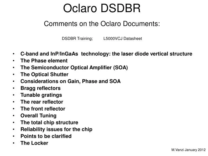
Oclaro DSDBR Comments on the Oclaro Documents: DSDBR Training; L5000VCJ Datasheet. C-band and InP/InGaAs technology: the laser diode vertical structure The Phase element The Semiconductor Optical Amplifier (SOA) The Optical Shutter Considerations on Gain, Phase and SOA Bragg reflectors

E N D
Oclaro DSDBRComments on the Oclaro Documents:DSDBR Training; L5000VCJ Datasheet • C-band and InP/InGaAs technology: the laser diode vertical structure • The Phase element • The Semiconductor Optical Amplifier (SOA) • The Optical Shutter • Considerations on Gain, Phase and SOA • Bragg reflectors • Tunable gratings • The rear reflector • The front reflector • Overall Tuning • The total chip structure • Reliability issues for the chip • Points to be clarified • The Locker M.Vanzi January 2012
C-band and InP/InGaAs technology: the laser diode vertical structure The C-band ranges from 191 to 196 THz, which corresponds to optical wavelengths (in vacuum) from 1570 to 1530 nm and to photon energies from 0.79 to 0.81 eV. The ternary compound In0.53Ga0.47As has its bandgap at 0.777 eV (at 300°K), that leads its spectrum for spontaneous emission (Eg Eg+2kT) to completely embrace the C-band. On the other side, this ternary compound is perfectly matched to the InP lattice, which allows for growing In0.53Ga0.47As by epitaxy on an InP substrate. Moreover, the higher bandgap of InP itself (1.27 eV at 300°K) makes InP perfectly suitable for building the confinement layers of a laser diode with its active layer made of that ternary compound. See my report: List of failure modes and mechanisms in Laser Diodes part 1/2. Appendix 2. Epitaxial rules for DH lasers
The Phase element .1 The same structure may act as a phase element, provided: • Light enters the element from outside at frequency n • No reflection exists at entrance and exit sides • A low, independent, forward current is allowed to flow InGaAs InP InGaAs light The injected current changes the charge density The charge density changes the refractive index n The phase change Df across the distance L is InP InP Low current= no gain= absorption= attenuation L
The Phase element .2 A gain and a phase element can then be combined within a single monolithic structure phase current laser current mirror mirror phase gain
The Phase element .3 mirror mirror mirror mirror • Phase change is equivalent to a change in the cavity length. • Spectrum envelope unchanged • Multimode operation survives • Modes shift with phase change • Mode spacing changes
The Phase element .4 Fine tuning of the Oclaro phase element spans a 50 GHz range, that is equivalent to the minimum separation between C-band channels 191 THz 196 THz C-band channels
The Semiconductor Optical Amplifier (SOA) The same structure may act as an Optical Amplifier, provided: • Light enters the element from outside at frequency n • No reflection exists at entrance and exit sides • A high, independent, forward current is allowed to flow InGaAs InP InGaAs light High current= gain= no absorption= amplification InP The SOA is not a laser itself only because of the absence of its own resonant cavity It is a pumped element as for fiber amplifiers Anyway it also introduces a phase shift, because of the current injection It does not affect modality: even multimodes are equally amplified. InP L
The Optical Shutter As for the phase element, at low current the SOA attenuates light because of optical absorption. This property is used enabling even reverse bias of the SOA, that turns itself into a highly absorbing element, that is an optical shutter
Considerations on Gain, Phase and SOA.1 Two slides about… wrong solutions
Considerations on Gain, Phase and SOA.2 A hypothetic structure SOA current phase current laser current mirror mirror phase Amplifier/shutter gain Such a structure is: tunable and gain controllable, BUT multimodal and with SOA affecting phase control
Considerations on Gain, Phase and SOA.3 Another hypothetic structure SOA current laser current phase current mirror mirror phase amplifier gain Such a structure would avoid SOA interference on phase control BUT is not feasible in monolithic technology. And remains multimodal
Considerations on Gain, Phase and SOA.4 • For tunability across the whole C-band one needs: • Single mode selection • Tunability 100 times wider than the range of the phase element • Cavity resonance • Gain flattening, if tuning affects gain • Monitoring of power and frequency The first two requirements ask for tunablegratings
Bragg reflectors .1 ng nc tail na nc Moving wavefront They are made of corrugated layers, with proper diffraction index, in the vicinity of the active layer. Apart from corrugation, the structure is the same as for the gain element waveguide light The “tails” of the optical wave, extending outside the active layer, sense the corrugation as an effective modulation of the refractive index along the waveguide Effective index along the waveguide
Bragg reflectors .2 Any index variation acts on the propagating wave as an impedance variation for an electric signal. Reflected waves are originated at any corrugation point. They can interfere positively (strong reflection) or negatively (null reflection), depending on l. The shape of the corrugation defines the reflection function R as a function of l. The reflection function is related to the Fourier transform of the grating function Proper patterning of the grating allows for “R(l) engineering”
Tunable gratings .1 ng nc na nc Tuning current As for the phase element, when a given forward current is fed across the structure, the overall refractive index of the waveguide is multiplied by a constant factor. That is equivalent to change l=l0/n That is, in turn, equivalent to stretch the grating, and then to change the reflection function R(l) In order to span the whole C-band, the tuning should change l by some 3%. This is excessive.
Tunable gratings .2 phase rear Bragg reflector 6a a Assuming a similar width of the ridge, the contact area on the rear Bragg reflector is about 6 times the area of the phase element. On the other side, the maximum current fed into the latter is 60 mA, while in the former is 10. This means a similar maximum injected density of charges, and then a similar tuning range.
The rear reflector .1 In order to allow for full C-band coverage, the Oclaro rear Bragg reflector is designed to produce 7 peaks (supermodes), spaced of some 6-7 nm. Tuning will allow any wavelength in the C-band to be centered by at least one peak. S band C band L band
The rear reflector .2 Total shift of the “comb reflection” It remains only to select the supermode, that is the specific peak shift of a single peak
The front reflector .1 The front reflector is made of a chirped grating. It is made of a continuously varying pitch, that produces a broad, uniform reflection across the wole C-band. rear Bragg reflector front reflector
The front reflector .2 Tuning When two adjacent contacts are fed by current, the effective local pitch is modified. This changes the reflection function, depleting some reflected wavelengths and enhancing others. A broad peak forms, able to select a single supermode 8 metal contacts, operated in pairs tuned front reflector rear Bragg reflector front reflector
Overall Tuning Continuous tuning Supermode selection
The total chip structure ISOA AR AR The total structure is then full integrated into a single monolithic element
Reliability issues for the chip • Advantages: • No movable parts • Full internal cavity (no interfaces in open air) • Only one thermal control needed • No local mirrors (no COD) • Disadvantages: • Many corrugated epitaxial interfaces: risk of defect growth • Rather high operating currents for rear reflector, coupled with corrugation • Absorbing elements: need for a SOA (further current)
Points to be clarified • Vertical structure (TEM required) • Details of gratings (very many FIB-TEM required, in several locations) • Material analysis 1. The bent ridge in the SOA sections calls for a laterally confined optical guide. A BH solution is expected (see List of Failures part 1) 2.1 The rear grating, in order to give a comb reflection, is expected to be a sampled structure 2.2 The front grating, in order to give a wide flat reflection, is said to be a linearly chirped structure. This should be verified.
The Locker .1 Beamsplitter PD - 1 Transmit Primary beam PD - 2 l Transmit( ) The locker elements are slightly rotated in order to avoid unwanted resonance between back reflections. Split l Reflection( ) Photodiode (Rx) P Etalon Photodiode (Tx) The Etalon has a transmission function T given by (see my document: The Double Etalon …) that implies nd 3 mm Where The reflection function R is its complement to unit: Their ratio is It is useful to note that the beam reflected by the Etalon undergoes another splitting (dashed line) when crossing the splitter. This means that PD2 does not read the full reflection of the Etalon. Anyway, being the splitter weakly reflecting, in order to save power in the primary beam, or the attenuation at PD2 is neglected, or is compensated by upscaling the PD2 reading.
The Locker .2 Ch 49 Ch 50 The Oclaro documents indicate the ratio R/T as determining the frequency, and the sum R+T as monitoring the total power. About power, it is clear that the sum R+T is proportional to the intensity of the transmitted primary beam. About frequency, Oclaro plots the difference T-R instead of the ratio R/T. The following graph plots everything. A value F=2 has been assumed in order to fit the original drawing. In any case, the 100GHz channels result perfectly tuned at the maxima and minima of the four curves The utility of the ratio R/T is that tunes the 50GHz channels exactly at midway of the descending or ascending nearly linear parts of the curve (where the intensity read by the two photodiodes is equal).