Download
1 / 8
140 likes | 464 Views
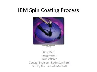
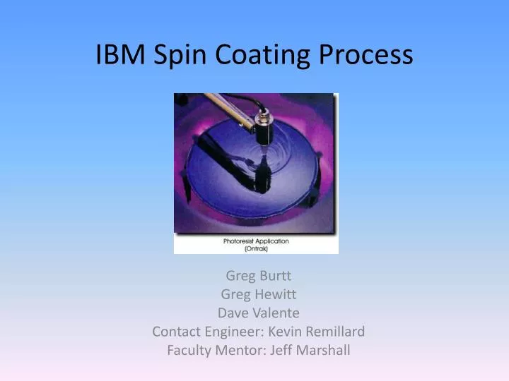
IBM Spin Coating Process. Greg Burtt Greg Hewitt Dave Valente Contact Engineer: Kevin Remillard Faculty Mentor: Jeff Marshall. Typical Photolithography Process. IBM’s Problem. During the spin coating process, defects sometimes appear on the wafer.

E N D
IBM Spin Coating Process Greg Burtt Greg Hewitt Dave Valente Contact Engineer: Kevin Remillard Faculty Mentor: Jeff Marshall
IBM’s Problem • During the spin coating process, defects sometimes appear on the wafer. • Damage to the bowl from handling and cleaning have also been spotted as a cause of the defects. • A cleaning process must be run a few times a day to remove built up resist from the “bowl set” (a 3-part set of plastic pieces that houses the silicon wafer being coated and collects the excess applied chemicals) in order to reduce the probability of defects. • This cleaning process involves the use of a cleaning disk and a solvent to attempt to remove as much resist as possible from the bowl, but it is incapable of removing all of the build-up. • Consequently, the bowl set must be removed every two weeks and trucked to a company that cleans them. This is a very costly process for IBM for a few reasons. • There is a lot of down-time involved in removing and replacing the bowls, this is time translates directly to lost money because of decreased productivity. • They must also pay to have the bowls trucked to a facility and to have them cleaned there. • Some bowl sets come back with damage and need to be replaced.
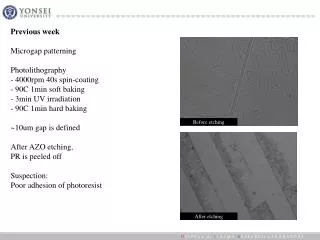
Defect Description • Wafer defects are thought to be caused by the loss of proper air flow through the bowl setup. • Very small particles (“ball bearings”) of resist become suspended in the air during the normal application process, the flow ideally carries all these particles away from the wafer surface into a drain. • In some cases, the flow becomes disrupted allowing these particles to return from the air to the wafer surface. Alternatively, the flow picks up new ball bearings from the sides of the bowl and deposits them on the wafer surface. Either instance results in a defect on the wafer. • IBM believes, and we will assume their conclusion is correct, that in an otherwise undamaged bowl, these defects are primarily caused by a build-up of dried resist on the bowl surfaces.
Goal Our goal is to reduce the cost to IBM of maintenance and upkeep of the bowl sets by altering the coating or cleaning process. Thereby allowing bowls to be changed less often, reducing cleaning costs and the risk of damage during handling. Two fundamentally different approaches can be taken. • Airflow: To decrease the sensitivity of the spin-coating process to imperfections in the bowl such as dried resist. • Material and Cleaning: To reduce the ability of the resist to collect on the sides of the bowl in volumes that have a detrimental effect on the spin-coating process.
Two Testing Options Airflow Buildup of Resist If the resist buildup path is chosen, the experimental setup can be greatly simplified. The bowl set and chamber would be used mainly to characterize the resist buildup and test cleaning disk designs and process changes. Material and coating ideas would be tested on samples obtained from manufacturers. Parameters such as contact angles could be measured and compared. Resist could also be applied and dried onto the samples, then the ease of removal could be assessed experimentally. • If the airflow path on the flow chart is taken, a full experimental setup must be created. The flow velocity, angular velocity of the wafer, and internal geometry of the photoresist application machine must be accurately replicated. This would allow us to make alterations to the velocity, knife edge, roughness, and bowl geometry and test their effects. This would be done with a mix of computer simulation and visual observation using suspended particles such as what would be found in smoke or the vapors of dry ice.
Constraints • Process chemicals cannot be changed • Wafer spin speed is variable, so a solution must accommodate any angular velocity up to a maximum of several thousand RPMs • IBM prefers that the bowl geometry remain unchanged • Exhaustive testing would have to result • Cost to IBM can not increase • This includes the cost associated with bowl manufacture and cleaning as well as equipment down-time for cleaning and bowl changes