Download
1 / 11
110 likes | 229 Views
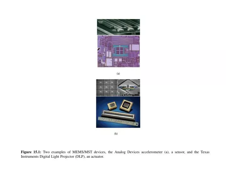
Figure 15.1: Two examples of MEMS/MST devices, the Analog Devices accelerometer (a), a sensor, and the Texas Instruments Digital Light Projector (DLP), an actuator. Figure 15.2: Example of deposition (a), lithography (b), etching(c).

E N D
Figure 15.1: Two examples of MEMS/MST devices, the Analog Devices accelerometer (a), a sensor, and the Texas Instruments Digital Light Projector (DLP), an actuator.
Figure 15.2: Example of deposition (a), lithography (b), etching(c).
Figure 15.3: Example of interconnects in an integrated circuit generated by deposition, lithography, etc. (Reproduced with kind permission of IBM, http://www.chips.ibm.com/news/sa27.html).
Figure 15.4: Example of bulk micromachine process for a pressure sensor.
Figure 15.5: Example of surface micromachine process for an accelerometer.
Figure 15.6: Plot of the total number of transistors shipped by Intel by year from 1968 to 2002.(Reproduced with kind permission of Intel, http://www.intel.com/research/silicon/mooreslaw.htm)
Figure 15.7: Drawing of the CMOS last approach developed by Sandia National Labs13 (Reproduced with kind permission of Sandia National Laboratories, http://www.sandia.gov/mstc/technologies/micromachines/overview.html).Projector (DLP), an actuator.
Figure 15.8: Photograph of Multiple Gear Speed Reduction Unit fabricated in Sandia’s SUMMiT MEMS process (Reproduced with kind permission of Sandia National Laboratories, SUMMiTTM Technologies, http://mems.sandia.gov/scripts/images.asp).
Figure 15.9: Photograph of the dual axis convective accelerometer by MEMSIC. (Reproduced with kind permission of MEMSIC, Inc., http://www.memsic.com/memsic/).
Figure 15.10: Scanning electron micrograph of electrostatically actuated resonator from the ASIMPS process. (Reproduced with kind permission of G. Fedder).
Figure 15.11: Areas of growth for MEMS and MST technologies. (From MEMS 1999 Emerging Applications and Markets by permission of System Planning Corporation.)