Download
1 / 2
20 likes | 157 Views
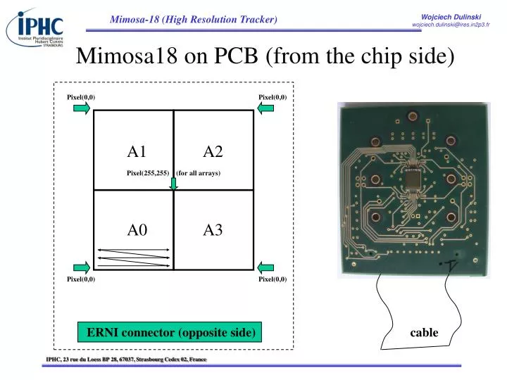
Mimosa18 on PCB (from the chip side). Pixel(0,0). Pixel(0,0). A1. A2. Pixel(255,255) (for all arrays). A0. A3. Pixel(0,0). Pixel(0,0). ERNI connector (opposite side). cable. 4 matrix of 256*256 pixel. Self-bias No radiation Tolerant pixel. Noise optimized.

E N D
Mimosa18 on PCB (from the chip side) Pixel(0,0) Pixel(0,0) A1 A2 Pixel(255,255) (for all arrays) A0 A3 Pixel(0,0) Pixel(0,0) ERNI connector (opposite side) cable
4 matrix of 256*256 pixel. • Self-bias No radiation Tolerant pixel. • Noise optimized. • High precision tracking pixel • This sensors have been designed and fabricated for • this application using AMS 0.35 OPTO process. • Single sensor consists of 512x512 pixel array with • a pitch of 10 µm, providing an active area of 5x5 mm2 • fabricated using standard (14 µm thick epitaxy) • and experimental (20 µm epitaxy)