Download
1 / 62
990 likes | 1.75k Views
Chapter 4 CMOS Process Technology. Boonchuay Supmonchai Integrated Design Application Research ( IDAR ) Laboratory July 5th, 2004; Revised - June 26th, 2006. Outlines. Chip-Making Process Photolithography CMOS IC Fabrication Processes Simple Process Modern Process Packaging Technology.

E N D
Chapter 4CMOS Process Technology Boonchuay Supmonchai Integrated Design Application Research (IDAR) Laboratory July 5th, 2004; Revised - June 26th, 2006
Outlines • Chip-Making Process • Photolithography • CMOS IC Fabrication Processes • Simple Process • Modern Process • Packaging Technology CMOS Process Technology
Packaging Crystal Growth Chip-Making Process: An Overview Photolithography CMOS Process Technology
From Smithsonian, 2000 Growing the Silicon Ingot • Most common technique is the Czochralski (CZ) method developed by Mitsubishi Materials Silicon in the 50’s • Length: up to 2 m • Diameter: 200 mm (8”) to 300 mm (12”) • Weight: Over 225 kg. • Pulling takes up to hundred hours CMOS Process Technology
Develop by Mitsubishi in the 50’s Czochralski (CZ) Method • Crystal orientation is determined by seed orientation • Ingot diameter is determined by temperature, orientation, and extraction speed. 1420 C CMOS Process Technology
Ingot is cut around and ground down into a uniform diameter (8”-12”), then sliced into wafers of about 1 mm thick. Wire Saw Machine The sliced wafers are mechanically lapped by the use of alumina abrasive material to remove surface roughness and damages caused by the saw cut and to improve the flatness of the wafer. Lapping Machine Wafer Shaping CMOS Process Technology
Mechanical damages induced during the previous processes are removed by chemical etching. The mechano-chemical polishing process improves the flatness of the wafer, making highly flat surface by the use of colloidal silica. Wafer Polishers Wafer Shaping (2) CMOS Process Technology
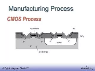
N Well V DD V DD PMOS 2l PMOS Contacts In Out Out In Metal 1 NMOS Polysilicon Layout Schemetic NMOS GND The Target: CMOS Inverter CMOS Process Technology
Current CMOS Structure CMOS Process Technology
Define active areas Etch and fill trenches Implant well regions Deposit and pattern polysilicon layer Implant source and drain regions and substrate contacts Create contact and via windows Deposit and pattern metal layers CMOS Process at a Glance • One full photolithography sequence per layer (mask) • Built (roughly) from the bottom up 5 metal 2 4 metal 1 2 polysilicon 3 source and drain diffusions 1tubs (aka wells, active areas) CMOS Process Technology
liquid carrier with a suspended abrasive component such as aluminum oxide or silica From Smithsonian, 2000 Planarization: Polishing the Wafers CMP (Chemical-Mechanical Planarization) - Essential to keep the surface of the wafer approximately flat between processing steps. CMOS Process Technology
Outlines • Chip-Making Process • Photolithography • CMOS IC Fabrication Processes • Simple Process • Modern Process • Packaging Technology CMOS Process Technology
Photolithography • An IC consists of several layers of material that are manufactured in successive steps. Photo + Litho + Graphy (Light) (Stone) (Writing) =“Writing Stone with Light” • Photolithographyis used to selectively process the layers, where the 2-D mask geometry is copied on the surface. CMOS Process Technology
oxide growth photoresist coating Photolithographic Process optical mask stepper exposure photoresist removal (ashing) Typical operations in a single photolithographic process process step Ion implantation Plasma etching Metal deposition photoresist development acid etch spin, rinse, dry CMOS Process Technology
Oxide Growth/Oxide Deposition • Oxidation of the silicon surface creates a SiO2 layer that acts as an insulator. • Oxide layers are also used to isolate metal interconnections. An annealing step is required to restore the crystal structure after thermal oxidation. CMOS Process Technology
Photoresist Deposition/Coating • The surface of the wafer is coated with a photosensitive material, the photoresist. • The mask pattern is developed on the photoresist, with UV light exposure. • Depending on the type of the photoresist (negative or positive), the exposed or unexposed parts of the photoresist change their property and become resistant to certain types of solvents. CMOS Process Technology
A Mask Sample Stepper Exposure • Glass Mask (reticle) containing the patterns to be transferred is brought in close proximity to the wafer • The mask pattern is developed on the photoresist, with UV light exposure. CMOS Process Technology
Photoresist Devolopment • The wafers are developed in either an acid or base solution to remove the nonexposed (exposed) areas of the photoresist. • Once the exposed photoresist is removed, the wafer is “soft baked” at a low temperature to harden the photoresist. CMOS Process Technology
Etching is a common process to pattern material on the surface. Once the desired shape is patterned with photoresist, the unprotected areas are etched away. Acid Etching CMOS Process Technology
Spin, Rinse, and Dry • A special tool called SRD is used to clean the wafers after each acid etch step • Use de-ionized water to remove any residue chemical substance. • Use nitrogen because it has no reaction with the silicon. CMOS Process Technology
Various Process Steps • The exposed area can now be subjected to a wide range of process steps • Ion implantation • Plasma (Dry) etching • Metal (Thin Film) deposition CMOS Process Technology
Ashing - Photoresist Removal • A high-temperature plasma is used to selectively remove the remaining photoresist without damaging previous layers. • After ashing the wafer is ready for the next round of photolithography. CMOS Process Technology
Si-substrate UV-light Patterned optical mask Silicon base material Exposed resist SiO2 Si-substrate Si-substrate 3. Stepper exposure 1. After oxidation heat Exposed resist Photoresist SiO2 Si-substrate Si-substrate 4. Photoresist Devolop and Bake 2. After deposition of negative photoresist Photolithographic Process Example CMOS Process Technology
Chemical or plasma etch Hardened resist SiO 2 Si-substrate 5. After development and etching of resist, chemical or plasma etch of SiO2 Hardened resist SiO2 Si-substrate SiO2 6. After etching and spin, rinse and dry. Si-substrate 8. Final result after removal of resist (ashing) Photolithographic Process Example • Step 7 is optional in this example. The step is need only in implanting a well or doping polysilicon • Planarization step is applied at least once in a cycle of photolithography CMOS Process Technology
Diffusion:Wafer is exposed to gas containing dopant under high temperature (900-1100 C) 1000 C Ion Implantation:A beam of dopant ions is swept over the surface - causing damage to substrate, need annealing Purified Ion beam Diffusion and Ion Implantation • Change the electrical characteristics of silicon locally by adding doping agents to the exposed area. • The dopant ions penetrate the surface with a penetration depth that is proportional to their kinetic energy. CMOS Process Technology
Outlines • Chip-Making Process • Photolithography • CMOS IC Fabrication Processes • Simple Process • Modern Process • Packaging Technology CMOS Process Technology
Photolithography Masks • Each photolithography step during fabrication must be defined by a separate photolithography mask. • Each mask layer must be drawn (either manually or using a design automation tool) according to the layout design rules. • The combination (superposition) of all necessary mask layers completely defines the circuit to be fabricated. CMOS Process Technology
Layout Design Rules • To allow reliable fabrication of each structure, the mask layers must conform to a set of geometric layout design rules. • Usually, the rules (for example: minimum distance and/or separation between layers) are expressed as multiples of a scaling factor - • lambda () - minimum resolution of a technology • For each different fabrication technology, lambda factor can be different. CMOS Process Technology
Examples of Layout Design Rules A Minimum-Sized Transistor CMOS Process Technology
More Example of Layout Rules CMOS Process Technology
1. Create thin oxide in the “active” regions, thick elsewhere 2. Deposit polysilicon 3. Etch thin oxide from active region (poly acts as a mask for the diffusion) 4. Implant dopant(see previous slides) Self-Aligned Process CMOS Process Technology
Notes on Self-Aligned Process • Polysilicon gate is patterned before source and drain are created, • Thereby defining the precise location of the channel region and the locations of the source and drain regions relative to the gate. • And consequently reducing parasitic capacitances in the transistor. • However, this technique cannot completely stop lateral diffusion • Accounts for difference between drawn transistor dimensions and actual ones. CMOS Process Technology
cut line p well Simplified CMOS Inverter Process CMOS Process Technology
P-Well Mask CMOS Process Technology
Active Mask CMOS Process Technology
Poly Mask CMOS Process Technology
Self-Aligned Gate P+ Select (Source/Drain) Mask CMOS Process Technology
Self-Aligned Gate N+ Select (Source/Drain) Mask CMOS Process Technology
Contact Mask CMOS Process Technology
Metal Mask CMOS Process Technology
Outlines • Chip-Making Process • Photolithography • CMOS IC Fabrication Processes • Simple Process • Modern Process • Packaging Technology CMOS Process Technology
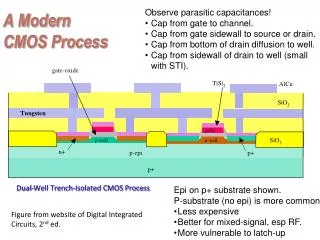
Dual-Well Trench-Isolated CMOS gate oxide field oxide Al (Cu) SiO2 TiSi2 tungsten SiO2 p well n well p-epi n+ p+ Trench p- A Modern CMOS Process Both n- and p- wells grown on top of an epitaxial layer (using trench isolation areas of SiO2) CMOS Process Technology
p-epi Base material: p+ substrate with p-epi layer + p Si N 3 4 SiO After deposition of gate-oxide and sacrificial nitride (acts as a buffer layer) 2 p-epi + p After plasma etch of insulating trenches using the inverse of the active area mask p + Modern CMOS Process Walk-Through CMOS Process Technology
SiO 2 After trench filling, CMP planarization, and removal of sacrificial nitride n After n-well and VTp adjust implants p After p-well and VTn adjust implants Modern CMOS Process Walk-Through (2) CMOS Process Technology
poly(silicon) After polysilicon deposition and etch n + + p After n+ source/drain and p+ source/drain implants. These steps also dope the polysilicon. SiO 2 After deposition of SiO2 insulator and contact hole etch Modern CMOS Process Walk-Through (3) CMOS Process Technology
Al After deposition and patterning of first Al layer. Al SiO 2 After deposition of SiO2 insulator, etching of via’s, deposition and patterning of second layer of Al. Modern CMOS Process Walk-Through (4) CMOS Process Technology
State-of-the-Art Example CMOS Process Technology
Interconnect Delay Crisis • As technology shrinks, interconnect delay has more and more impact on the overall design performance. • Wire delay now accounts for > 40% of total delay in a circuit • There are 2 key points where interconnect delay can be reduced. • Use low-resistivity material • Copper in stead of Aluminum (what is the best conductor?) • Use insulator material with a lower dielectric constant (k) than SiO2 (Reduce coupling) CMOS Process Technology
Advanced Metallization CMOS Process Technology
Insulator (SiO2) Transistor Silicon-on-Insulator (SOI) • The idea is to construct the transistor structures in a very thin layer of silicon on an insulating material rather than a common substrate as in bulk CMOS process. • This reduces parasitic capacitances and eliminates substrate noise coupling. CMOS Process Technology