Download
1 / 19
190 likes | 355 Views
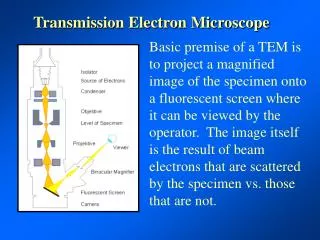
Diffraction in the Transmission Electron Microscope Vidhya Sagar Jayaseelan. TEM- What is it?. Advantages of TEM. High Resolution images 1,000,000 X Sub-micron level diffraction Defect imaging – dislocations, twins, stacking faults, point defects, antiphase boundaries

E N D
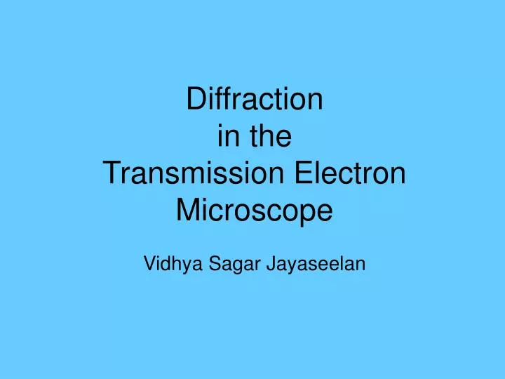
Diffraction in the Transmission Electron MicroscopeVidhya Sagar Jayaseelan
Advantages of TEM • High Resolution images 1,000,000 X • Sub-micron level diffraction • Defect imaging – dislocations, twins, stacking faults, point defects, antiphase boundaries • Simultaneous imaging, structural and compositional analysis • Orientation studies possible • Identifying the phases and crystal structures • Site occupancy of atoms/ions
Disadvantages of TEM • Sample size • Preparation • Instrument issues • Operation • Interpretation
Wavelength of electrons Wavelength – magnification q*U = ½ mv2,λ = h/ (m * v ) where: λ = wavelength h = Planck's constant (6.6 X 10⁻²⁷) m = mass of the electron (9.1 X 10⁻²⁸) v = velocity of the electron U = Potential drop λ = (1.23 nm)/ U1/2
Electron Sample Interaction Incident electron beam Backscattered electrons-Elastic Inelastic- Secondary electrons Characteristic X rays Auger Electrons 2θ Inelastic scattering Elastic scattering-Diffraction Transmitted beam
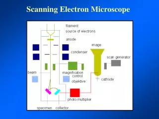
Optics of the TEM • Gun • Lenses • Focal length • Apertures • Screen
Image Contrast in TEM • Thickness • Composition • Atomic number/phases • Diffraction (orientation) • Strain fields • Fringe Effects
Diffraction in TEM Reciprocal lattice –What is it? Equations- Bragg, Laue, Fourier Transform Real Reciprocal Ewald Sphere
Zone axis for SC <100> <100> <110> <111>
Real to Reciprocal lattice equations The relationship • Bragg’s law nλ = 2d sinθ • Laue equation r = (S-S0) / λ • Fourier Transform F(s) = ∫ dx f(x) exp(–i2πsx) Structure factor Fhkl = ∑ fn exp { 2πi (hx1 +ky1+ lz1)}
TEM Diffraction- What can we infer? • Phases and crystal structure types • Crystal symmetry and space group • Orientation relationships between phases • Determining growth directions, interface coherency • Identifying defects , i.e. twinning, SFs, Dislocations • Ordering behavior of crystal structures and the site occupancy preferences
Kikuchi lines Inelastic scattering without significant wavelength change leads to formation of Kikuchi lines by diffraction. Incoming beam has every possible direction. Outgoing strong beam is at Bragg angle. This is particularly seen in thick samples θ
More…. • Transmission Electron Microscopy- Dr. Vasudevan’s Graduate Course • Transmission Electron Microscopy – David B. Williams and C. Barry Carter • Transmission Electron Microscopy – Ludwig Reimer • WWW