Download
1 / 15
150 likes | 346 Views
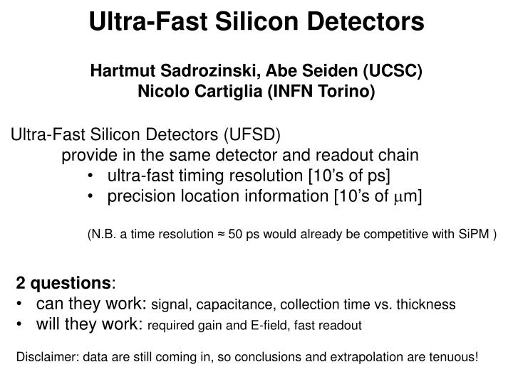
Ultra-Fast Silicon Detectors Hartmut Sadrozinski, Abe Seiden (UCSC) Nicolo Cartiglia (INFN Torino). Ultra-Fast Silicon Detectors (UFSD) provide in the same detector and readout chain ultra-fast timing resolution [10’s of ps] precision location information [10’s of m m]

E N D
Ultra-Fast Silicon DetectorsHartmut Sadrozinski, Abe Seiden (UCSC) Nicolo Cartiglia (INFN Torino) • Ultra-Fast Silicon Detectors (UFSD) • provide in the same detector and readout chain • ultra-fast timing resolution [10’s of ps] • precision location information [10’s of mm] • (N.B. a time resolution ≈ 50 ps would already be competitive with SiPM ) • 2 questions: • can they work: signal, capacitance, collection time vs. thickness • will they work: required gain and E-field, fast readout • Disclaimer: data are still coming in, so conclusions and extrapolation are tenuous!
Motivation • Up to now, semiconductor sensors have supplied precision data only for the 3 space dimensions (diodes, strips, pixels, even “3D”), while the time dimension has had limited accuracy (e.g. to match the beam structure in the accelerator). • We believe that being able to resolve the time dimension with ps accuracy would open up completely new applications not limited to HEP • An example in HEP are forward physics projects at the LHC, like the AFP. Scattered protons are tracked from stations 100’s of meters downstream back to the interaction region and the z-vertex is determined from the timing information. So good position resolution and excellent timing are required, which at the moment is done with different detector technologies (pixels and Micro-channel plates. • Proposal: Combined-function pixel detector will collect electrons from thin n-on-p pixel sensors read out with short shaping time electronics • Charge multiplication with gain g increases the collected signal • Need very fast pixel readout
UFSD Pixel Collected Charge Signal = thickness*EPM Collection time = thickness/vsat (vsat = 80mm/ns) Realistic gain & cap Good time resolution For thickness > 5 um, Capacitance to the backplane Cb << Cint For thickness = 2 um, Cb ~ ½ of Cint, and we might need bipolar (SiGe)?
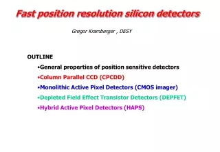
Fast charge collection: Drift Velocity and E-Field Gregor Kramberger, 19th RD50 Workshop As long as E-field E > 20kV/cm drift velocity vdrift = vsat ≈ 80mm/ns Full Depletion Voltage VFD [V] Bias Voltage for Emin =20kV/cm
Charge multiplication (CM) in silicon sensors (discovered by RD50 institutions) might have applications beyond off-setting charge lost due to trapping during the drift of electrons or holes. • Charge multiplication makes silicon sensors similar to drift chambers (DC) or Gas Micro-strip Detectors (GMSD), where a modest number of created charges drift to the sense wire, are amplified there (by factors of > 104) and are then used for fast timing. • We propose considering silicon detectors for simultaneous precision position and fast timing measurements. • Recall our experience with DC: Need to balance the need of high E-field around a wire to have charge multiplication with the need to keep the E-field low to prevent breakdown (wire diameter, field shaping wires,.) and give proper drift field The drifting electrons contribute mainly to the collected charge after they have undergone charge multiplication, which means that the pulse develops (in principle) in a short time. But the very large charge density in the “plasma cloud” prevents the electron to move until the ions have drifted away! So electron signal given by hole dynamics!? • Basic question for use of CM What field strength do we need? Can the sensor geometry and doping profile engineered so that the amplification field can be kept high, but just below the breakdown field? Benefits of Gain in Detectors
Estimate of pulse shape from Ramo Timing with falling edge?
Anna Macchiolo, 16th RD50 Workshop Barcelona “Avalanche” needs distance to develop, but here l ≤ 10mm! Require max and min E-field close to breakdown field (270kV/cm)
Bias Voltages to reach maximum E-fieldlarge over-voltage required (diode)
E-Field across a pixel Anna Macchiolo, 16th RD50 Workshop Barcelona
Strip Depletion depth y0 y0 chosen so that: Solve numerically: Drift charge through the field, get signal using Ramo’s theorem: (simulation programs written by G. Kramberger) Simplified simulation of strip sensors, real E-field variation not as bad because the hole current injection stabilizes the field but even 30% difference (Elena)is bad At Vbias < Vfd: Example of electric field: Ф = 1.6·1015 n/cm2, U = 900 V Ey(V/µm) 10 I. Mandić, RESMDD08, Florence, Italy, 15th -17th October 2008
E-Field across a pixel will vary , resulting in different gains in the center and the edges. To make use of E-field close to breakdown requires uniformity across pixel
Epi, short drift distances and planar diode gives g = 6.5 Using red laser and a’s probes E-field and gainclose to the junction, where it counts.Diode gives uniformity
What about fast readout: • CERN fixed-target experiment (NA62) needs very fast pixel sensors: Gigatracker (GTK) • Prototype CFD system (INFN Torino) has ~ 100 ps resolution, predicted to be 30 ps in next iteration. • Optimized for 200mm sensors and hole collection (?), could it be re-designed for electron collection from 2 – 10mm sensors?
Summary and more questions: • Thin pixel sensors with moderate gain could give time resolution between 10 and 100 ps. • Epi diodes seem perform adequately (g=6.5). How can we engineer a pixel sensor to have a uniform field across the pixel like a planar diode? Graded doping concentration? Special deep implants? Trenches? • How much can we over-deplete pixel sensors to raise Emin? • Do we need irradiated sensors, or can we use low-ohmic sensors with field shaping? • Charge multiplication increases after long annealing (Igor, Marco), could this be employed? • Start making thin epi strip sensors • Extend simulations to very thin sensors! • Need to collaborate with chip designers.
Back-upE-Field, Depletion Voltage, Resistivity, Thickness • Assumptions: • Desired signal charge 2000 e- • Observed Gain: • irradiated 3D sensors: g ≈ 3.5 (Freiburg), • irradiated epi diodes g = 6.6 (Hamburg) • gain > 20 unrealistic? • N-on-p pixels (collect electrons) • Pixel area A = 50 um x 50 um • Electron yield EPM = 80 e-/um • Saturated drift velocity vsat = 180 um/ns • Breakdown field EB ≈ 270 kV/cm • Full depletion Voltage VFD = cons*d2/rho cons = 0.0113, d in um, rho in kOhm-cm • Max Efield at depletion Emax = 2*VFD/d • Max Efield at Bias Voltage V Emax = (V+VFD)/d • Min Efield at Bias Voltage V Emax = (V-VFD)/d • Capacitance to backplane Cb = A/d • Capacitance to neighbors Cint ≈ 200 fF