Download
1 / 65
650 likes | 881 Views
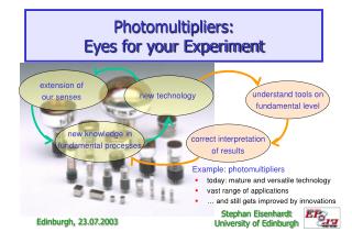
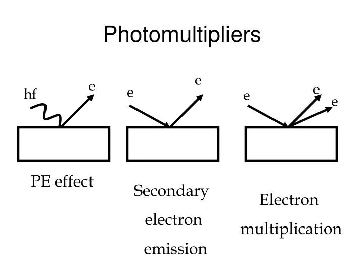
Photomultipliers. e. e. e. e. hf. e. e. PE effect. Secondary electron emission. Electron multiplication. hf. e. Anode. Dynode. -V. Photomultiplier tube. Combines PE effect with electron multiplication to provide very high detection sensitivity Can detect single photons.

E N D
Photomultipliers e e e e hf e e PE effect Secondary electron emission Electron multiplication
hf e Anode Dynode -V Photomultiplier tube • Combines PE effect with electron multiplication to provide very high detection sensitivity • Can detect single photons.
Microchannel plates • The principle of the photomultiplier tube can be extended to an array of photomultipliers • This way one can obtain spatial resolution • Biggest application is in night vision goggles for military and civilian use
Microchannel plates • MCPs consist of arrays of tiny tubes • Each tube is coated with a photomultiplying film • The tubes are about 10 microns wide http://hea-www.harvard.edu/HRC/mcp/mcp.html
MCP array structure http://hea-www.harvard.edu/HRC/mcp/mcp.html
MCP fabrication http://hea-www.harvard.edu/HRC/mcp/mcp.html
Disadvantages of Photomultiplers as sensors • Need expensive and fiddly high vacuum equipment • Expensive • Fragile • Bulky
Photoconductors • As well as liberating electrons from the surface of materials, we can excite mobile electrons inside materials • The most useful class of materials to do this are semiconductors • The mobile electrons can be measured as a current proportional to the intensity of the incident radiation • Need to understand semiconductors….
Evac Ec Ef Ev Metal Photoelecric effect with Energy Bands Evac Ef Semiconductor Band gap: Eg=Ec-Ev
To amplifier e Ec Evac Ef Ev Semiconductor Photoconductivity
Photoconductors • Eg (~1 eV) can be made smaller than metal work functions f (~5 eV) • Only photons with Energy E=hf>Eg are detected • This puts a lower limit on the frequency detected • Broadly speaking, metals work with UV, semiconductors with optical
Band gap Engineering • Semiconductors can be made with a band gap tailored for a particular frequency, depending on the application. • Wide band gap semiconductors good for UV light • III-V semiconductors promising new materials
5m Example: A GaN based UV detector This is a photoconductor
Choose the material for the photon energy required. • Band-Gap adjustable by adding Al from 3.4 to 6.2 eV • Band gap is direct (= efficient) • Material is robust
Stimulated emission E2 - E1 = hf E2 E1 Two identical photons Same - frequency - direction - phase - polarisation
Lasers • LASER - acronym for • Light Amplification by Stimulated Emission of Radiation • produce high intensity power at a single frequency (i.e. monochromatic)
Principles of Lasers • Usually have more atoms in low(est) energy levels • Atomic systems can be pumped so that more atoms are in a higher energy level. • Requires input of energy • Called Population Inversion: achieved via • Electric discharge • Optically • Direct current
Population inversion Lots of atoms in this level N2 Energy N1 Few atoms in this level Want N2 - N1 to be as large as possible
Population Inversion (3 level System) E2 (pump state), t2 ts >t2 E1 (metastable- state), ts Pump light hfo Laser output hf E1 (Ground state)
Light Amplification • Light amplified by passing light through a medium with a population inversion. • Leads to stimulated emission
Laser • Requires a cavity enclosed by two mirrors. • Provides amplification • Improves spectral purity • Initiated by “spontaneous emission”
Laser Cavity • Cavity possess modes • Analagous to standing waves on a string • Correspond to specific wavelengths/frequencies • These are amplified
Properties of Laser Light. • Can be monochromatic • Coherent • Very intense • Short pulses can be produced
Types of Lasers • Large range of wavelengths available: • Ammonia (microwave) MASER • CO2 (far infrared) • Semiconductor (near-infrared, visible) • Helium-Neon (visible) • ArF – excimer (ultraviolet) • Soft x-ray (free-electron, experimental)
Optical Fibre Sensors • Non-Electrical • Explosion-Proof • (Often) Non-contact • Light, small, snakey => “Remotable” • Easy(ish) to install • Immune to most EM noise • Solid-State (no moving parts) • Multiplexing/distributed sensors.
Applications • Lots of Temp, Pressure, Chemistry • Automated production lines/processes • Automotive (T,P,Ch,Flow) • Avionic (T,P,Disp,rotn,strain,liquid level) • Climate control (T,P,Flow) • Appliances (T,P) • Environmental (Disp, T,P)
Optical Fibre Principles Cladding: glass or Polymer Core: glass, silica, sapphire TIR keeps light in fibre Different sorts of cladding: graded index, single index, step index.
Optical Fibre Principles • Snell’s Law: n1sin1=n2sin2 • crit = arcsin(n2/n1) • Cladding reduces entry angle • Only some angles (modes) allowed
Phase and Intensity Modulation methods • Optical fibre sensors fall into two types: • Intensity modulation uses the change in the amount of light that reaches a detector, say by breaking a fibre. • Phase Modulation uses the interference between two beams to detect tiny differences in path length, e.g. by thermal expansion.
Intensity modulated sensors: • Axial displacement: 1/r2 sensitivity • Radial Displacement
Microbending (1) Microbending • Bent fibers lose energy • (Incident angle changes to less than critical angle)
Microbending (2): Microbending • “Jaws” close a bit, less transmission • Give jaws period of light to enhance effect • Applications: • Strain gauge • Traffic counting
More Intensity modulated sensors Frustrated Total Internal Reflection: • Evanescent wave bridges small gap and so light propagates • As the fibers move (say car passes), the gap increases and light is reflected Evanescent Field Decay @514nm
More Intensity modulated sensors Frustrated Total Internal Reflection: Chemical sensing • Evanescent wave extends into cladding • Change in refractive index of cladding will modify output intensity
Disadvantages of intensity modulated sensors • Light losses can be interpreted as change in measured property • Bends in fibres • Connecting fibres • Couplers • Variation in source power
Phase modulated sensors Bragg modulators: • Periodic changes in refractive index • Bragg wavelenght (λb) which satisfies λb=2nD is reflected • Separation (D) of same order as than mode wavelength
Phase modulated sensors • Multimode fibre with broad input spectrum • Strain or heating changes n so reflected wavelength changes • Suitable for distributed sensing Period,D λb=2nD
Temperature Sensors • Reflected phosphorescent signal depends on Temperature • Can use BBR, but need sapphire waveguides since silica/glass absorbs IR
Phase modulated sensors Fabry-Perot etalons: • Two reflecting surfaces separated by a few wavelengths • Air gap forms part of etalon • Gap fills with hydrogen, changing refractive index of etalon and changing allowed transmitted frequencies.
Digital switches and counters • Measure number of air particles in air or water gap by drop in intensity • Environmental monitoring • Detect thin film thickness in manufacturing • Quality control • Counting things • Production line, traffic.
NSOM/AFM Combined Bent NSOM/AFM Probe • Optical resolution determined by diffractionlimit (~λ) • Illuminating a sample with the "near-field" of a small light source. • Can construct optical images with resolution well beyond usual "diffraction limit", (typically ~50 nm.) SEM - 70nm aperture
NSOM Setup • Ideal for thin films or coatings which are several hundred nm thick on transparent substrates (e.g., a round, glass cover slip).