Download
1 / 61
620 likes | 785 Views
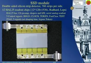
SSD upgrade. M. LeVine, R. Scheetz BNL Ch. Renard , S. Bouvier Subatech H. Matis , J. Thomas LBNL. HFT components. HFT. SSD IST PXL. IFC Inner Field Cage. FGT. Magnet Return Iron. TPC Volume. EAST. WEST. Solenoid. SSD. SSD characteristics. SSD ladder.

E N D
SSD upgrade M. LeVine, R. ScheetzBNL Ch. Renard, S. BouvierSubatech H. Matis, J. Thomas LBNL
HFT components HFT SSD IST PXL IFC Inner Field Cage FGT Magnet Return Iron TPC Volume EAST WEST Solenoid
SSD expected lifetime in RHIC • Radiation expected during 12 weeks of 500 GeVp-p running: 3.4 krad • Extrapolated from measurements in STAR IR • Lifetime limit of SSD silicon+associated (on ladder) electronics: >200 krad • Based on measurements of SSD module in 20 MeV proton beam • Radiation limit: >30 years of p-p running
SSD upgrade scope • Improve readout performance • Change mechanical mounting to improvehermiticity and interface with IDS • Improve reliability of air cooling
SSD readout upgrade • SSD electronics -- designed to read out at 200 Hz • New STAR DAQ now reads up to 1 kHz with low dead time • SSD must conform to the new performance standard
Readout upgrade concept • Reading out front end: • Replace single ADC with 16 ADCs • digitize 16 modules in parallel • Increase sampling rate to 5.00 MHz • All ladders processed concurrently • Transferring data to PC • Increase link throughput to DAQ PC to 120 Mbyte/s per 5 ladders • 1850 µs -> 450 µs • Multiple (derandomizing) buffers effectively hides this time • Dead time: 11%@750Hz, <2%@100Hz • [cf. existing: >80%@750Hz,30% @ 100Hz] 2.5 ms -> 154 µs
Readout components Ladder cards RDO (1 of 8) Slave FPGA VME FPGA VME interface Fiber links Slave FPGA Slave FPGA DAQ PC Master FPGA DAQ interface DDL SlaveFPGA TRG interface SlaveFPGA South platform VME crate Outer support cone DAQ room
Data formats • non zero-suppressed • 3 10-bit ADC values to a 32-bit word • Fixed order: position in buffer/word -> geographical position of strip • zero suppressed • Only strips with ADC value above threshold are present • ADC value (10 bits) + strip location (14 bits) • One strip per 32-bit word • Alleviates large memory access burden on DAQ PC • Doing this in real time in FPGA is simple
Ladder data path 20 16 40 MHz 50 MHz 5 MHz 80 MHz module 16 bit width32 words deep adc 12bit 16 bit serial output X16 packer serializer to fiber FIFO 2 JTAG TDOs 80 MHz 5 MHz module Write enable:true on 10 clocks only adc 12bit 16 bit serial output 1 set of adc samples: 10 X 16 bits => repacked into: 2 X 4 X 20 bits
FIFO1 1:10 deserialize FIFO2 mux 10 10 FIFO3 FIFO4 RDO slave - unpacker • unpacking 4 20-bit words to 5 16-bit words word 1 JTAG TDOs 40 MHz word 2 5 MHz 2 deserialize 50 MHz 50 MHz word 3 demux FIFO 20 x16 x16 first wd word 4 16 bit word 5 20 bit
Slave FPGA – ADC processing - - + + ADC 1 1 2 3 write ped address write ped data 1 2 3 ADC 16 14 10 counter 0-767 (no zero suppression) Packing register Pedestal memory Buffer 0..3 256X32 bits 10 Subtract/ multiplex 1 from unpacker remainder Readout to master FPGA Pedestal memory Buffer 0..3 256X32 bits 10 Subtract/ multiplex 16 read address read address mode address 8 ÷ 3 2 10 Mode: ADC, pedestal, or difference Select: ADC, pedestal only, or max(difference,0) Pedestal write
Dead time calculations – zero suppression 3 % occupancy
Status: slave FPGA • Components chosen • Altera Cyclone III EP3C55 • FPGA code largely finished • Functional simulations complete • Post P&R done for subsystems • Full place and route in progress
Status: ladder board • Analog • Level shifter (mux replacement) • Serial ADC (16 inputs instead of 1) • Digital • Serial ADC • Event control • Data packer • SerDes • GBIC • 4 temperature monitors • Slow control (JTAG) • Debug (USB interface) • Status - layout of PCB complete
Ladder board PCB Flex circuit layer
Testing road map • Ladder board standalone test • JTAG header to program FPGA for testing • Use USB interface to verify/correct FPGA behavior up to serdes • RDO standalone test • VME interface to program, probe master, slaves • Use user-defined JTAG to verify, debug • Integrate ladder, RDO with fiber • Entire system can be tested w/o DAQ PC • Use VME to communicate with master FPGA
New SSD ladder arrangement Cooling plenum
SSD services LV/HV (no HV out West) No Cooling out West Air Taken from IFC Volume Optical Data/Control Module Connectors (internal) Chordal Gaps Between FGT And WSC Shell Low Voltage Power in On Both Sides HV East Side Only Air Coolant (suction) East End Only
System overview North Platform DAQ Room Cooling The SSD is mounted on the OSC DAQ Computers SSD WSC ESC South Platform (RDO & Power) RDO LV/HV PS
SSD cooling • Replace Vortex blower (76 kW) • Use maintainable vacuum • Reroute tubing • Instrument with temperature and flow measurements
New developments • Measured analog response at ADCs • Single event upsets and remediation • Improved zero-suppression • Integration issues being addressed • Cables, fibers, routing, grounding • Safety issues (grounding, floating PS, fuses, HV)
Analog response vs clock frequency 4.3 MHz 5.0 MHz 6.0 MHz Horiz:100 ns/cm
Single event upsets • Ionizing radiation causes single bit errors in configuration memory (internal to FPGA) • Change FPGA behavior • Scale from observed error frequency in TOF • Estimate 1 error per 10 minutes in SSD • Must pro-actively detect these errors by running CRC checks while acquiring data
Improvement to zero suppression • Zero suppression based on preserving above-threshold strips • Want to retain neighbors as well • Problem: strips are not read out in order • Have to store them in intermediate buffer, in geographic order, before suppression • RAM has been added (larger FPGA) • Implementation will come later
Integration issues • Power cables will be Cu-coated Al • Cables to West (through FGT) are the most difficult due to limited area • Routing details being addressed • Grounding plan being integrated with other HFT subdetectors
Safety issues • Need to ensure that details will be approved by RHIC safety committee • Floating PS with safety resistors • Fuse protection forsense wires • HV considerations • HV is <100V, I < 0.1ma
SSD - summary • Design progressing well • Costs have been accurately estimated • Risks are minimal • No technical risks • Mitigation strategies in place
Spare slides Spare slides
Existing readout configuration • 1 ADC reads 16 modules sequentially • ADC sampling speed: 3 MHz • Connection to RDO is via copper cable • Restricts RDO location to magnet face • 1 RDO serves 10 ladders • Data link to DAQ computer oversubscribed Performance of existing system: • Dead time @100 Hz: 30% • Dead time @ 750 Hz: >80%
Slow controls • Path from RDO to ladder defined • JTAG transported on fiber pair • Multiple paths from VME CPU to RDO possible: • FP JTAG connector • Compatible with existing software, hardware • Provides migration path • VME interface • Best performance • Requires software development
Cost details for SSD readout • RDO card (qty: 10) • Components $3080 • Fabrication $ 910 • Assembly $ 910 • Total (each card) $4900 • Ladder card (qty: 50) • Components $1920 • Fabrication $1250 • Assembly $ 300 • Total (each card) $3470 • DDL links (qty: 12) • SIU $ 670 • ½ DRORC $ 840 • Total (per link) $1510 • DAQ PC (qty: 2) • Each $2900 • Total production cost: • $246.2K • Includes spares • Costs are burdened • Does not include prototypes
Data formats: zero suppressed • Only strips with ADC value above threshold are present • ADC value (10 bits) + strip location (14 bits) • One strip per 32-bit word • Alleviates large memory access burden on DAQ PC • Doing this in real time in FPGA is simple
Data flow: Ladder card • Each yellow box (x5) represents one ladder • Connection card + ADC card • Dual input ADC (x8) with bit-serial outputs • 16 outputs feed 1 gigabit serializer • Green boxes: readout card • Connection to readout card • gigabit fiber pair per ladder
Dataflow: Readout card • Per ladder (5X): • Optical link • Deserializer • Slave FPGA • 1 master FPGA • Manages data from the ladder FPGAs • Manages the DDL connection to the DAQ PC • Manages connection to TRG