Download
1 / 1
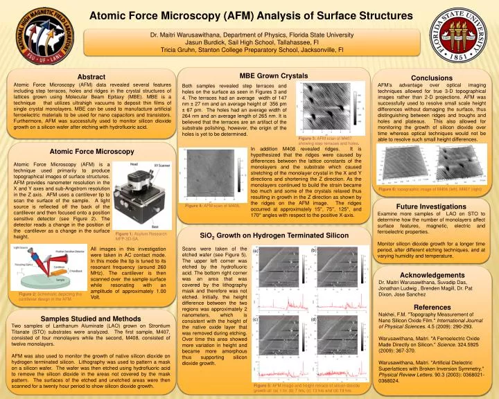
20 likes | 229 Views
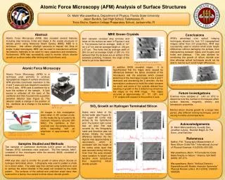
Atomic Force Microscopy (AFM) Analysis of Surface Structures. Dr. Maitri Warusawithana, Department of Physics, Florida State University Jasun Burdick, Sail High School, Tallahassee, Fl Tricia Gruhn, Stanton College Preparatory School, Jacksonville, Fl. MBE Grown Crystals. Conclusions

E N D
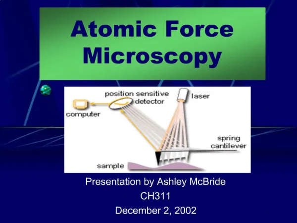
Atomic Force Microscopy (AFM) Analysis of Surface Structures Dr. Maitri Warusawithana, Department of Physics, Florida State University Jasun Burdick, Sail High School, Tallahassee, Fl Tricia Gruhn, Stanton College Preparatory School, Jacksonville, Fl MBE Grown Crystals Conclusions AFM’s advantage over optical imaging techniques allowed for true 3-D topographical images rather than 2-D projections. AFM was successfully used to resolve small scale height differenceswithout damaging the surface, thus distinguishing between ridges and troughs and holes and plateaus. This also allowed for monitoring the growth of silicon dioxide over time whereas optical techniques would not be able to resolve such small height differences. Abstract Atomic Force Microscopy (AFM) data revealed several features including step terraces, holes and ridges in the crystal structures of lattices grown using Molecular Beam Epitaxy (MBE). MBE is a technique that utilizes ultrahigh vacuums to deposit thin films of single crystal monolayers. MBE can be used to manufacture artificial ferroelectric materials to be used for nano capacitors and transistors. Furthermore, AFM was successfully used to monitor silicon dioxide growth on a silicon wafer after etching with hydrofluoric acid. Both samples revealed step terraces and holes on the surface as seen in Figures 3 and 4. The terraces had an average width of 147 nm ± 27 nm and an average height of 356 pm ± 67 pm. The holes had an average width of 264 nm and an average length of 265 nm. It is believed that the terraces are an artifact of the substrate polishing, however, the origin of the holes is yet to be determined. Figure 3: AFM scan of M407 showing step terraces and holes. Atomic Force Microscopy In addition M408 revealed ridges. It is hypothesized that the ridges were caused by differences between the lattice constants of the monolayersand the substrate which caused stretching of the monolayer crystal in the X and Y directions and shortening the Z direction. As the monolayerscontinued to build the strain became too much and some of the crystals relaxed thus resulting in growth in the Z direction as shown by the ridges on the AFM image. The ridges occurred at approximately 15°, 75°, 125°, and 170° angles with respect to the positive X-axis. Atomic Force Microscopy (AFM) is a technique used primarily to produce topographical images of surface structures. AFM provides nanometer resolution in the X and Y axes and sub-Angstrom resolution in the Z axis. AFM uses a cantilever tip to scan the surface of the sample. A light source is reflected off the back of the cantilever and then focused onto a position sensitive detector (see Figure 2). The detector reads a change in the position of the cantilever as a change in the surface height. Figure 6: topographic image of M408 (left), M407 (right) Future Investigations Examine more samples of LAO on STO to determine how the number of monolayers affect surface features, magnetic, electric and ferroelectric properties. Monitor silicon dioxide growth for a longer time period, after different etching techniques, and at varying humidity and temperature. Figure 4: AFM scan of M408. SiO2Growth on Hydrogen Terminated Silicon Figure 1: Asylum Research MFP-3D-SA. Scans were taken of the etched wafer (see Figure 5). The upper left corner was etched by the hydrofluoric acid. The bottom right corner was an area that was covered by the lithography mask and therefore was not etched. Initially, the height difference between the two regions was approximately 2 nanometers, which is consistent with the height of the native oxide layer that was removed during etching. Over time this area showed more variation in height and became more amorphous thus supporting silicon dioxide growth. All images in this investigation were taken in AC contact mode. In this mode the tip is tuned to its resonant frequency (around 260 MHz). The cantilever is then scanned over the sample surface while resonating with an amplitude of approximately 1.00 Volt. (b) (a) Acknowledgements Dr. MaitriWarusawithana, Suvadip Das, Jonathan Ludwig , Brenden Magill, Dr. Pat Dixon, Jose Sanchez References Nakhei, F.M. "Topography Measurement of Nano Silicon Oxide Film." International Journal of Physical Sciences. 4.5 (2009): 290-293. Warusawithana, Maitri. "A Ferroelectric Oxide Made Directly on Silicon." Science. 324.5925 (2009): 367-370. Warusawithana, Maitri. "Artificial Dielectric Superlattices with Broken Inversion Symmetry." Physical Review Letters. 90.3 (2003): 0368021-0368024. Figure 2: Schematic depicting the cantilever design in the AFM. Samples Studied and Methods Two samples of Lanthanum Aluminate (LAO) grown on Strontium Titanate (STO) substrates were analyzed. The first sample, M407, consisted of four monolayers while the second, M408, consisted of twelve monolayers. AFM was also used to monitor the growth of native silicon dioxide on hydrogen terminated silicon. Lithography was used to pattern a mask on a silicon wafer. The wafer was then etched using hydrofluoric acid to remove the silicon dioxide in the areas not covered by the mask pattern. The surfaces of the etched and unetched areas were then scanned for a twenty hour period to show silicon dioxide growth. (c) (d) Figure 5: AFM image and height retrace of silicon dioxide growth at: (a) 1 hr, (b) 7 hrs, (c) 13 hrs and (d) 19 hrs.