Download
1 / 22
220 likes | 360 Views
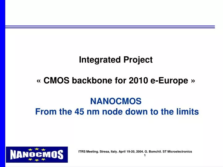
Integrated Project « CMOS backbone for 2010 e-Europe » NANOCMOS From the 45 nm node down to the limits. OUTLINE. European context Project objectives Consortium Project Structure Details of the work program Conclusions. N ANO C MOS European Context.

E N D
Integrated Project « CMOS backbone for 2010 e-Europe » NANOCMOS From the 45 nm node down to the limits
OUTLINE • European context • Project objectives • Consortium • Project Structure • Details of the work program • Conclusions
NANOCMOS European Context • Integrate in a coherent structure Cooperative European R§D projects and in the field of NANOCMOS Integrated Circuits. • Make a substantial contribution to optimize European efforts in Microelectronics in particular between Frame Work Programme 6Information Society Technology (IST) projects funded by the European Commission and MEDEA+ projects funded through the EUREKAmechanism.
1992 1993 1994 1995 1996 1997 1998 1999 2000 2001 2002 2003 2004 2005 ADEQUAT 0.35mm FE; 0.35mm BE ADEQUAT-1 ADEQUAT-2 0.25mm FE; 0.35mm BE ADEQUAT + COIN 0.18mm FE; 0.25mm BE ACE 0.18-0.15mm FE; 0.18mm BE DAMASCENE Copper inter. 100 nm FE HUNT MEDEA T201 90 nm Full Integr ARTEMIS 65 nm FE ULISSE Cu/low k 65 nm Full Integr. MEDEA T207 NESTOR 45/32/22 FE IST: 45 nm FE; 45 nm BE, 32/22, MEDEA: 45 nm Full Integr NANOCMOS European Technology Projects
NANOCMOS NANOCMOS 45 nm demonstration of feasibility 32/22 nm anticipation (European Commission) STREPS NEO: SINANO NANOCMOS 45 nm CMOS-300 Full CMOS Process Integration (MEDEA+)
NANOCMOS TECHNICAL OBJECTIVES • Achieve a demonstration of feasibility of a 45 nm CMOS logic process Q3/Q4 2005(IST Project) and a first full CMOS integration in a 300 mm industrial facility in 2007 (MEDEA+ project). • NANOCMOS planning allows time for further work to achieve maturity of a 45nm industrial process. Fits with 2003 ITRS Roadmap predictions/criteria for the 45 nm node “product shipment” in 2010. • Start the R§D activities on materials and process for a demonstration of feasibility of a 32 nm CMOS logic process in 2007. • Start the R§D activities on materials and process aiming the 22 nm node, in close cooperation with a Network of Excellence (SINANO) gathering more 50 European Universities /Institutes research teams.
INITIAL CONSORTIUM IC MANUFACTURERS ST Microelectronics Crolles § Agrate(F, I), PHILIPS Semiconductors Crolles(F), INFINEON(D) RESEARCH INSTITUTES § ACADEMIC TEAMS IMEC(B), CEA-LETI(F), PHILIPS ResearchLeuven(B) § Eindhoven(NTH) FHG(D, three centers), CNRS(F, eight laboratories), ZFM/TU Chemnitz(D) SMEs IBS(F), ISILTEC(D), MAGWELL(B), ACIES(F)
SUB PROJECT I: MATERIALS • WP I.1.1: Strained buffer layers • Thin SRBs (IMEC) • Relaxation mechanisms starting from pure Ge (CNRS, LETI) • STI process for SRBs (IMEC) • Strained Si on SRB: CMP, cleaning, doping, thermal stability (ST) • Integration(ST) • WP I.1.2: Strained Si on SiGeC • Epi re-growth of SiGeC with different C concentration (CNRS/IEF) • Growth of SiGeC with high C concentration gradient (ST, LETI) • WP I.1.3:Evaluation and characterization strained Si and relaxed SiGe • Identification and characterization of crystal defects (CNRS) • WP I.2.1: SOI for high mobility materials (LETI) • Growth of SiGeC on very thin SOI • WP I.1.2: Strained Si on SOI (IMEC) • Growth of ultra thin SRB on SOI (Ge condensation)
SUB PROJECT II: FEOL MODULES • WP II.1.1 High-k gate dielectrics (ST, LETI, FhG, IMEC, PHILIPS) • HfO2 and silicates based dielectrics by ALCVD and MOCVD • Interface, cleaning • Perovskite dielectrics formed by MBE(CNRS) • High-k formation via ion implantation (IBS) • WP II.1.2 Metal gate electrodes • MOCVD metal, ALD nitride based, PVD TaN (ST, LETI, IMEC, PHILIPS) • Dry etching (CNRS) • WP II.1.3 Surface preparation (IMEC, LETI) • WP II.2.1 S/D extensions • Low Rsq, <15 nm junctions: SPER, LTA (ST, LETI, IMEC, PHILIPS, CNRS) • Plasma immersion implantation (IBS) • WP II.2.2 Silicides and elevated source-drain • Scaling of NiSi (ST) • NiSi on elevated S/D. Applications to FD SOI (LETI, INFINEON) • NiSi of strained Si on SiGe( IMEC, PHILIPS)
SUB PROJECT III: New devices § architectures • WP III.1.1 Specifications of 45 nm planar devices (ST, PHILIPS, IMEC) • WP III.1.2 Integration of modules in bulk CMOS (ST, PHILIPS, IMEC) • Gate stack integration: benchmark high k vs oxynitride § poly vs metal gate • Shallow junctions integration • Strained silicon channel • Define “best” 45 nm compatible planar MOSFET • WP III.2.1 Novel devices for the 45 nm node (ST, INFINEON, LETI, CNRS, FhG) • Fully depleted thin Si on SOI § SON • Multigate devices: planar bonded DG MOS,FINFET, SON • WP III.2.2 Novel devices for the 32/22 nm nodes (ST, INFINEON, LETI, CNRS, FhG) • Double § triple gate, gate all around using FINFET § SON • Co integration with bulk CMOS
SUB PROJECT IV: Multilevel Metallization Modules • WP IV.1 Materials and process(ST/PHILIPS, IMEC, LETI, ZFM) • Nanoporous materials: CVD k<2.2, Spin on k<2.0 • Barrier materials: ALD WCN < 5 nm, self aligned barriers by electroless • WP IV.2 Dual Damascene architectures(PHILIPS, INFINEON, IMEC, LETI, ZFM, CNRS) • Advance patterning 80/80 nm, etching chemistries • Start air gap studies for the 32/22 nm nodes • WP IV.3 Modules integration(ST/PHILIPS, ST-I, IMEC, LETI, ZFM, ISILTEC) • Pore sealing: plasma treatments, liner deposition • Cu filling: seed repair for conformal PVD layer: • CMP: nearly damage free polish with spec uniformity, minimizing dishing, erosion,.. • Contact filling: high aspect ratio contacts, minimum barrier thickness by ALCVD dep. • WP IV.4 Reliability(ST/PHILIPS, PHILIPS, IMEC, LETI, ZFM) • Thermal properties • High frequency characterization • Electro migration Cu § Time dependent breakdown of dielectrics and barriers • WP IV.5 Extendibility and beyond Cu (ST/PHILIPS, PHILIPS, ST-I) • Ultra narrow lines/spaces(<80 nm) § contact/vias(<50 nm) • Wireless interconnects: integrated antenna, test structures
SUB PROJECT V: Process Characterization and Simulation • WP V.1. Process Characterization (ST/PHILIPS,PHILIPS,IMEC, LETI, CNRS) • Ultra shallow junctions, dielectrics Junctions down to 10 nm: SIMS, TOFSIMS, MEIS, AFM, SCM, SSRM, EHolography • Gate Stacks, dielectrics low k materials High k: HRTEM, EELS, EDX KPS Low k; IRSE, XRR, XR • Mechanical stress distributions Main approach UV Ramman Spectroscopy • WP V.2 Process simulation (ST, PHILIPS, INFINEON, CNRS, FhG, ZFM) • Support to technology development. • Implementation of models into available Software tools • Front end Process simulation • Back end Process simulation
SUB PROJECT VI: Device Characterization and Simulation • WP VI.1 Device simulation (ST, PHILIPS, INFINEON, CNRS) • Simulation for conventional architectures • Simulation for novel architectures • 45, 32 and 22 nm devices. TCAD with Monte Carlo and quantum codes • WP VI.2 Device modeling for circuit simulation (PHILIPS, MAGWEL) • Compact CMOS device models: for circuit simulators • Interconnect modeling and simulation • Signal propagation and interconnect delay simulations based on resolution -quasi static- of Maxwell equation • WP VI.3 Electrical characterization (PHILIPS, LETI, CNRS, FhG, MAGWEL) • Physical, electrical and reliability of dielectrics stacks • Electronic transport and mobility
SUB PROJECT VII: Equipment Modules • WP VII.1 Specifications and choice of applications (FhG, ST/PHILIPS) • Key applications: SiGe substrate, high k, silicides, CMP • Localized analysis areas • Plasma diagnostics • Large energy optical analysis • WP VII.2 Integrated metrology tools (FhG, ST/PHILIPS, IBS, ISILTEC) • Selection of sensors for processing tools • Integration into standard cluster ports
SUBPROJECT VIII: Device and MLM process integration. Validation test vehicle • WP VIII.1 Front end module integration (ST/PHILIPS, INFINEON, IMEC, FhG) • FE test mask vehicle:design • Simulation: targets HP,GP, LP. Compact models for SPICE • Device and SRAM cell Validation test vehicle • Back end module integration (ST/PHILIPS, IMEC, FhG) • BE test vehicle • Simulation • BE Validation test vehicle
SP VIII Objectives • 1st objective : Integration from SP III (FEOL) and SP IV (BEOL) in a unique process • 2nd objective : Validation of FEOL (SRAM cells) and BEOL (2 metal levels ) in 45nm technology • Global objective : provide a key-input for a CMOS045 full CMOS pricess integration in a 300 mm industrial facility
Design Rules Minimum pitch Shrink factor from 65nm rules Line/Space Active (nm) 140 0.74 60/80 Poly (nm) 135 0.75 45/90 Contact (nm) 160 0.76 70/90 Metal1 (nm) 135 0.75 70/65 Via-x (nm) 160 0.76 75/85 Metal-x (nm) 160 0.76 85/75 Poly-Contact distance (nm) 40 0.73 - N+/P+ distance (nm) 140 0.74 - 6 transistor SRAM cell (µm2) 0.35 1.86 Max Gate Density (MGate/mm²) 1.5 1.86 Tentative design rules for first test vehicle
1.2 1.2 Fujitsu Fujitsu /IEDM03 /IEDM03 TSMC/IEDM03 TSMC/IEDM03 1 1 ( ( specific specific layout layout ) ) Cell size [µm²] Cell size [µm²] 0.8 0.8 Crolles nanoCMOS nanoCMOS Toshiba/IEDM02 Toshiba/IEDM02 VLSI04 target target 0.6 0.6 Crolles/VLSI03 Crolles/VLSI03 0.4 0.4 Toshiba/VLSI03 Toshiba/VLSI03 (simulation) (simulation) 0.2 0.2 Samsung/IEDM03 Samsung/IEDM03 0 0 45nm 45nm node node 65nm 65nm node node 90nm 90nm node node 2001 2001 2003 2003 2005 2005 2007 2007 SRAM Bit celll size - NANOCMOS targets SRAM cell size 0.35-0.25 mm2
Design rules and technology validators • The design rules enables competitive validators for the 45nm on FE and BE in terms of SRAM bit-cells and 2 level metallization module • The design rules have been established by extrapolating historical and recent literature trends. • As the target cell sizes require pitches below 160nm – the lower limit of today’s 193nm lithography – the fabrication of the SRAM bit-cells will imply in the first phase of the project the use of e-beam lithography on several critical levels. • In parallel, 193nm-lithography should improve by the combination with immersion techniques. • For the SRAM bit-cell: four different layouts going from a “High Density Design” with a 0.334µm2 cell size down to a “Ultra-High Density Design” of 0.248µm2
Timing for FEOL/BEOL test vehicle Specs common SP8/SP3/SP4 Benchmark SRAM/MLM SP8 SRAM MLM DRM Test-mask Integration results t0 t0+6 t0+12 t0+18 t0+24 Researchresults Consolidated device results Specs common SP3/SP4/SP8 First test vehicle SP3/SP4
CONCLUSIONS • NANOCMOS addresses the main R§D challenges to improve performance and increase integration of logic CMOS Integrated Circuits within the time frame required by the ITRS Roadmap to introduce in production the 45 nm node and anticipate the 32 and 22 nm node generations. • First phase of NANOCMOS plans to demonstrate a representative test vehicle of the 45 nm node in 2005 from a first choice of an appropriate integration scheme among many device architectures and materials. • NANOCMOS would be followed by an industrial oriented project aiming Full 45 nm node logic CMOS process integration in 300 mm wafers. • In parallel a second phase of NANOCMOS will propose the demonstration of feasibility of a 32 nm node technology. • NANOCMOS partners will bring their experience to the ITRS working teams, to contribute to the worldwide consensus building process of a Roadmap as a source of guiding for the Semiconductor Industry.