Download
1 / 149
1.58k likes | 1.92k Views
ECE 271 Electronic Circuits I. Topic 8 Complementary MOS (CMOS) Logic Design. Chapter Goals. Introduce CMOS logic concepts Explore the voltage transfer characteristics of CMOS inverters Learn to design basic and complex CMOS logic gates Discuss the static and dynamic power in CMOS logic

E N D
ECE 271 Electronic Circuits I Topic 8Complementary MOS (CMOS) Logic Design NJIT ECE 271 Dr, Serhiy Levkov
Chapter Goals • Introduce CMOS logic concepts • Explore the voltage transfer characteristics of CMOS inverters • Learn to design basic and complex CMOS logic gates • Discuss the static and dynamic power in CMOS logic • Present expressions for dynamic performance of CMOS logic devices • Present noise margins for CMOS logic • Introduce design techniques for “cascade buffers” NJIT ECE 271 Dr, Serhiy Levkov
CMOS Inverter Technology • Complementary MOS, or CMOS, needs both PMOS and NMOS devices for the logic gates to be realized • The concept of CMOS was introduced in 1963 by Wanlass and Sah. • CMOS are more complicated in design and production, thus are more expensive to fabricate • Have not been widely used until the 1980’s as NMOS microprocessors started to dissipating as much as 50 W and more and alternative design technique was needed • CMOS dominate digital IC design today NJIT ECE 271 Dr, Serhiy Levkov
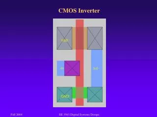
CMOS Inverter • Circuit schematic for a CMOS inverter • Simplified operation model with a high input applied • Simplified operation model with a low input applied NJIT ECE 271 Dr, Serhiy Levkov
CMOS Inverter • Circuit schematic for a CMOS inverter • Simplified operation model with a high input applied • Simplified operation model with a low input applied • When vI is pulled high (to VDD), the PMOS transistor is turned off, while the NMOS device is turned on pulling the output down to VSS NJIT ECE 271 Dr, Serhiy Levkov
CMOS Inverter • Circuit schematic for a CMOS inverter • Simplified operation model with a high input applied • Simplified operation model with a low input applied • When vI is pulled high (to VDD), the PMOS transistor is turned off, while the NMOS device is turned on pulling the output down to VSS • When vI is pulled low (to VSS), the NMOS transistor is turned off, while the PMOS device is turned on pulling the output up to VDD NJIT ECE 271 Dr, Serhiy Levkov
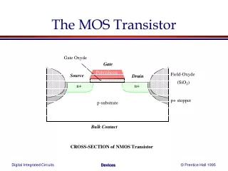
CMOS Inverter Technology • The CMOS inverter consists of a PMOS device stacked on top on an NMOS device, but they need to be fabricated on the same wafer • To accomplish this, the technique of “n-well” implantation is needed as shown in this cross-section of a CMOS inverter NJIT ECE 271 Dr, Serhiy Levkov
NMOS and PMOS recap NJIT ECE 271 Dr, Serhiy Levkov
NMOS and PMOS recap NJIT ECE 271 Dr, Serhiy Levkov
NMOS and PMOS recap NJIT ECE 271 Dr, Serhiy Levkov
NMOS and PMOS recap NJIT ECE 271 Dr, Serhiy Levkov
NMOS and PMOS recap NJIT ECE 271 Dr, Serhiy Levkov
NMOS and PMOS recap NJIT ECE 271 Dr, Serhiy Levkov
NMOS and PMOS recap NJIT ECE 271 Dr, Serhiy Levkov
NMOS and PMOS recap NJIT ECE 271 Dr, Serhiy Levkov
NMOS and PMOS recap NJIT ECE 271 Dr, Serhiy Levkov
NMOS and PMOS recap NJIT ECE 271 Dr, Serhiy Levkov
NMOS and PMOS recap NJIT ECE 271 Dr, Serhiy Levkov
Static States of the CMOS Inverter • The capacitor discharges through RonN , current exists only during discharge, no dc current exists. NJIT ECE 271 Dr, Serhiy Levkov
Static States of the CMOS Inverter • The capacitor discharges through RonN , current exists only during discharge, no dc current exists. NJIT ECE 271 Dr, Serhiy Levkov
Static States of the CMOS Inverter • The capacitor discharges through RonN , current exists only during discharge, no dc current exists. NJIT ECE 271 Dr, Serhiy Levkov
Static States of the CMOS Inverter • The capacitor discharges through RonN , current exists only during discharge, no dc current exists. NJIT ECE 271 Dr, Serhiy Levkov
Static States of the CMOS Inverter • The capacitor discharges through RonN , current exists only during discharge, no dc current exists. NJIT ECE 271 Dr, Serhiy Levkov
Static States of the CMOS Inverter • The capacitor discharges through RonN , current exists only during discharge, no dc current exists. NJIT ECE 271 Dr, Serhiy Levkov
Static States of the CMOS Inverter • The capacitor discharges through RonN , current exists only during discharge, no dc current exists. NJIT ECE 271 Dr, Serhiy Levkov
Static States of the CMOS Inverter • The capacitor discharges through RonN , current exists only during discharge, no dc current exists. NJIT ECE 271 Dr, Serhiy Levkov
Static States of the CMOS Inverter • The capacitor discharges through RonN , current exists only during discharge, no dc current exists. NJIT ECE 271 Dr, Serhiy Levkov
Static Characteristics of the CMOS Inverter • The capacitor discharges through RonN , current exists only during discharge, no dc current exists. • The capacitor charges through RonP , current exists only during charging, no dc current exists. NJIT ECE 271 Dr, Serhiy Levkov
Static Characteristics of the CMOS Inverter • The capacitor discharges through RonN , current exists only during discharge, no dc current exists. • The capacitor charges through RonP , current exists only during charging, no dc current exists. NJIT ECE 271 Dr, Serhiy Levkov
Static Characteristics of the CMOS Inverter • The capacitor discharges through RonN , current exists only during discharge, no dc current exists. • The capacitor charges through RonP , current exists only during charging, no dc current exists. NJIT ECE 271 Dr, Serhiy Levkov
Static Characteristics of the CMOS Inverter • The capacitor discharges through RonN , current exists only during discharge, no dc current exists. • The capacitor charges through RonP , current exists only during charging, no dc current exists. NJIT ECE 271 Dr, Serhiy Levkov
Static Characteristics of the CMOS Inverter • The capacitor discharges through RonN , current exists only during discharge, no dc current exists. • The capacitor charges through RonP , current exists only during charging, no dc current exists. NJIT ECE 271 Dr, Serhiy Levkov
Static Characteristics of the CMOS Inverter • The capacitor discharges through RonN , current exists only during discharge, no dc current exists. • The capacitor charges through RonP , current exists only during charging, no dc current exists. NJIT ECE 271 Dr, Serhiy Levkov
Static Characteristics of the CMOS Inverter • The capacitor discharges through RonN , current exists only during discharge, no dc current exists. • The capacitor charges through RonP , current exists only during charging, no dc current exists. NJIT ECE 271 Dr, Serhiy Levkov
Static Characteristics of the CMOS Inverter • The capacitor discharges through RonN , current exists only during discharge, no dc current exists. • The capacitor charges through RonP , current exists only during charging, no dc current exists. NJIT ECE 271 Dr, Serhiy Levkov
Static Characteristics of the CMOS Inverter • The capacitor discharges through RonN , current exists only during discharge, no dc current exists. • The capacitor charges through RonP , current exists only during charging, no dc current exists. NJIT ECE 271 Dr, Serhiy Levkov
CMOS Inverter – building VTC • To better understand what’s happening in inverter and to get the complete model we need to build the VTC - voltage transfer characteristics. NJIT ECE 271 Dr, Serhiy Levkov
CMOS Inverter – building VTC • To better understand what’s happening in inverter and to get the complete model we need to build the VTC - voltage transfer characteristics. • To construct VTC we use the load line method for different load states. NJIT ECE 271 Dr, Serhiy Levkov
CMOS Inverter – building VTC • To better understand what’s happening in inverter and to get the complete model we need to build the VTC - voltage transfer characteristics. • To construct VTC we use the load line method for different load states. • However, since the load in this case is also a nonlinear transistor, the “load line” approach will consist of superimposing I-Vcharacteristics of NMOS and PMOS transistors. NJIT ECE 271 Dr, Serhiy Levkov
CMOS Inverter – building VTC • To better understand what’s happening in inverter and to get the complete model we need to build the VTC - voltage transfer characteristics. • To construct VTC we use the load line method for different load states. • However, since the load in this case is also a nonlinear transistor, the “load line” approach will consist of superimposing I-Vcharacteristics of NMOS and PMOS transistors. • It requires that the I-V curves of the NMOS and PMOS devices are transformed onto a common coordinate set. NJIT ECE 271 Dr, Serhiy Levkov
CMOS Inverter – building VTC • To better understand what’s happening in inverter and to get the complete model we need to build the VTC - voltage transfer characteristics. • To construct VTC we use the load line method for different load states. • However, since the load in this case is also a nonlinear transistor, the “load line” approach will consist of superimposing I-Vcharacteristics of NMOS and PMOS transistors. • It requires that the I-V curves of the NMOS and PMOS devices are transformed onto a common coordinate set. • We select the input voltage VI NJIT ECE 271 Dr, Serhiy Levkov
CMOS Inverter – building VTC • To better understand what’s happening in inverter and to get the complete model we need to build the VTC - voltage transfer characteristics. • To construct VTC we use the load line method for different load states. • However, since the load in this case is also a nonlinear transistor, the “load line” approach will consist of superimposing I-Vcharacteristics of NMOS and PMOS transistors. • It requires that the I-V curves of the NMOS and PMOS devices are transformed onto a common coordinate set. • We select the input voltage VI, the output voltage VO NJIT ECE 271 Dr, Serhiy Levkov
CMOS Inverter – building VTC • To better understand what’s happening in inverter and to get the complete model we need to build the VTC - voltage transfer characteristics. • To construct VTC we use the load line method for different load states. • However, since the load in this case is also a nonlinear transistor, the “load line” approach will consist of superimposing I-Vcharacteristics of NMOS and PMOS transistors. • It requires that the I-V curves of the NMOS and PMOS devices are transformed onto a common coordinate set. • We select the input voltage VI, the output voltage VO , and the NMOS drain current IDNas the variables of choice. NJIT ECE 271 Dr, Serhiy Levkov
CMOS Inverter – building VTC • To better understand what’s happening in inverter and to get the complete model we need to build the VTC - voltage transfer characteristics. • To construct VTC we use the load line method for different load states. • However, since the load in this case is also a nonlinear transistor, the “load line” approach will consist of superimposing I-Vcharacteristics of NMOS and PMOS transistors. • It requires that the I-V curves of the NMOS and PMOS devices are transformed onto a common coordinate set. • We select the input voltage VI, the output voltage VO , and the NMOS drain current IDSNas the variables of choice. • The PMOS I-Vrelationship can be transformed as follows: • IDSp = –IDSn • VGSn = VI ; VGSp= VI – VDD • VDSn = VO ; VDSp= VO – VDD NJIT ECE 271 Dr, Serhiy Levkov
CMOS Inverter – building VTC • The I-Vcurves for NMOS are already plotted in the selected coordinate set Vin, Vout and IDN, so no change is needed. NJIT ECE 271 Dr, Serhiy Levkov
CMOS Inverter – building VTC • The I-Vcurves for NMOS are already plotted in the selected coordinate set Vin, Vout and IDN, so no change is needed. • The load-line curves of the PMOS device are obtained by a mirroring around the x-axisand a horizontal shift over VDD. NJIT ECE 271 Dr, Serhiy Levkov
CMOS Inverter – building VTC • The I-V curves for NMOS are already plotted in the selected coordinate set Vin, Vout and IDN, so no change is needed. • The load-line curves of the PMOS device are obtained by a mirroring around the x-axisand a horizontal shift over VDD. • This procedure is outlined below, where the subsequent steps to adjust the original PMOS I-V curves to the common coordinate set Vin, Vout and IDn are illustrated (in this example VDD = 2.5V. NJIT ECE 271 Dr, Serhiy Levkov
CMOS Inverter – building VTC • The I-V curves for NMOS are already plotted in the selected coordinate set Vin, Vout and IDN, so no change is needed. • The load-line curves of the PMOS device are obtained by a mirroring around the x-axisand a horizontal shift over VDD. • This procedure is outlined below, where the subsequent steps to adjust the original PMOS I-V curves to the common coordinate set Vin, Vout and IDn are illustrated (in this example VDD = 2.5V. NJIT ECE 271 Dr, Serhiy Levkov
CMOS Inverter – building VTC • Now we can superimpose the load curves of the PMOS on the IV curves of the NMOS. • For a dc operating points to be valid, the currents through the NMOS and PMOS devices must be equal. Graphically, this means that the dc points must be located at the intersection of corresponding load lines. • Some of those points (for Vin = 0, 0.5, 1, 1.5, 2, and 2.5 V) are marked on the graph. NJIT ECE 271 Dr, Serhiy Levkov
CMOS Inverter – building VTC • All operating points are located either at the high or low output levels. • The VTC of the inverter hence exhibits a very narrow transition zone. • This results from the high gain during the switching transient, when both NMOS and PMOS are simultaneously on, and in saturation. • In that operation region, a small change in the input voltage results in a large output variation. NJIT ECE 271 Dr, Serhiy Levkov